Lab 6 - ECE 421L
Authored
by John Huang.
Huangj19@unlv.nevada.edu
October 19, 2014
In this lab we will learn how to create a NAND gate, XOR gate and a full adder using these two gates.
We are using 6u/600u NMOS and PMOS for these gates.
2-input NAND gate schematic.
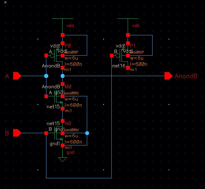
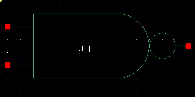
We use this schematic to create a symbol for the NAND.
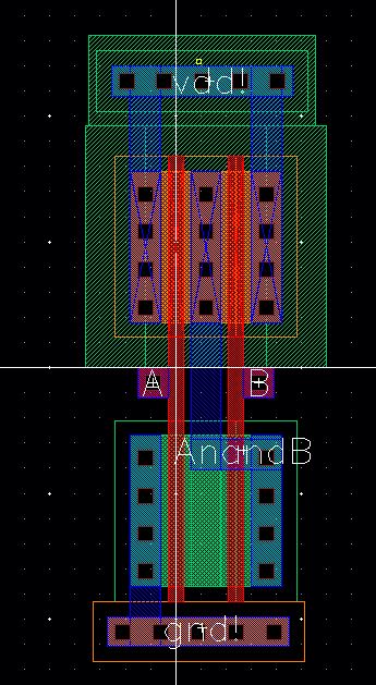
The
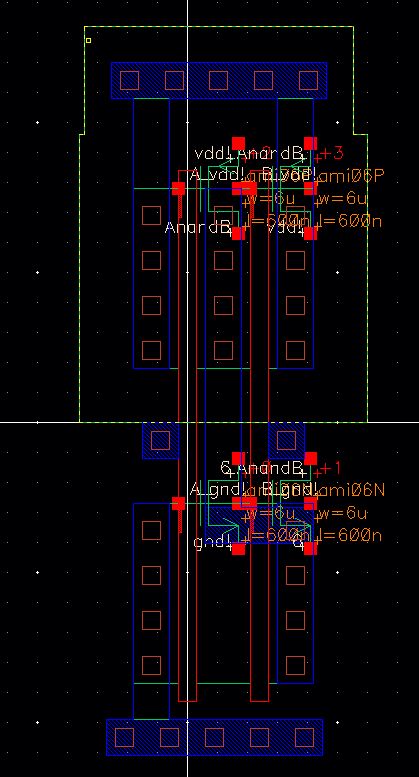
layout of our NAND gate. Very simple layout, we conneted the two NMOS
and PMOS by overlapping the gate of the PMOS and the gate of the NMOS.
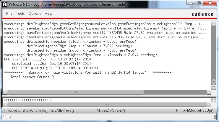
Passing the DRC for the layout.
The extracted view of our NAND layout.
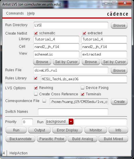
We can LVS the extracted layout with our schematic shown earlier.
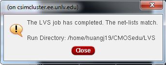
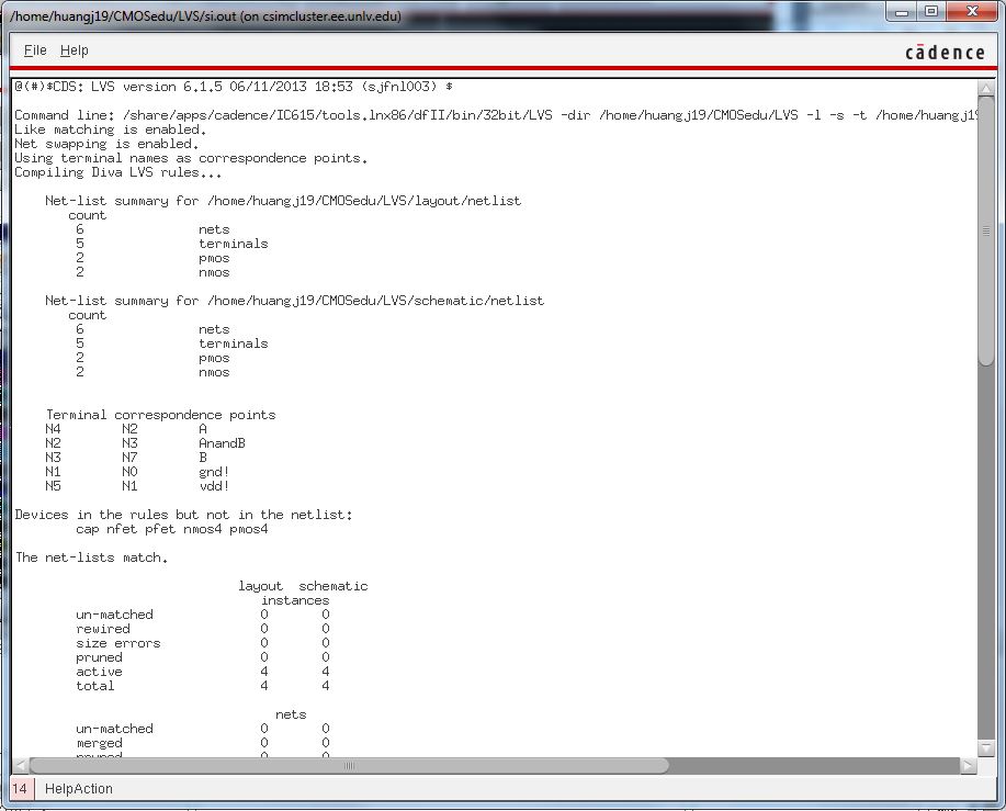
Matching netlist for the schematic and extracted layout.
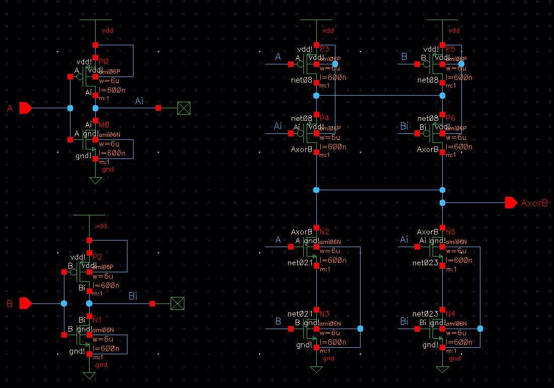
XOR gate schematic.
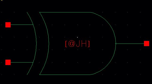
Creating a symbol from the schematic.
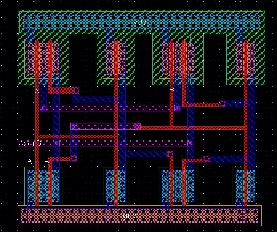
Layout of our XOR gate.
Because the layout of the XOR gate is a bit complicated, I had to use metal 2 to make some of the connections.
This was done using via from m2_m1 and also some m1_poly contacts.
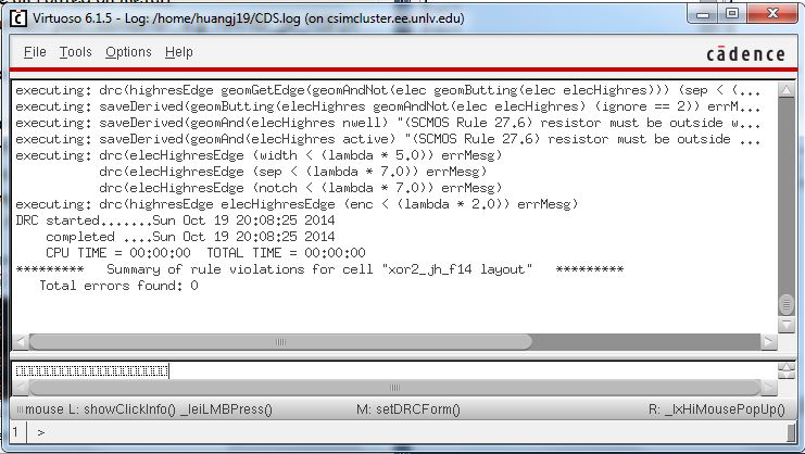
Making sure our layout passes our DRC.
Extracted layout of our XOR gate.
LVS the extracted layout and the schematic we created.
We can now test the NAND and the XOR gates we created.
We can use a simple schematic using the NAND, XOR and the 12u/6u inverter from the last lab.
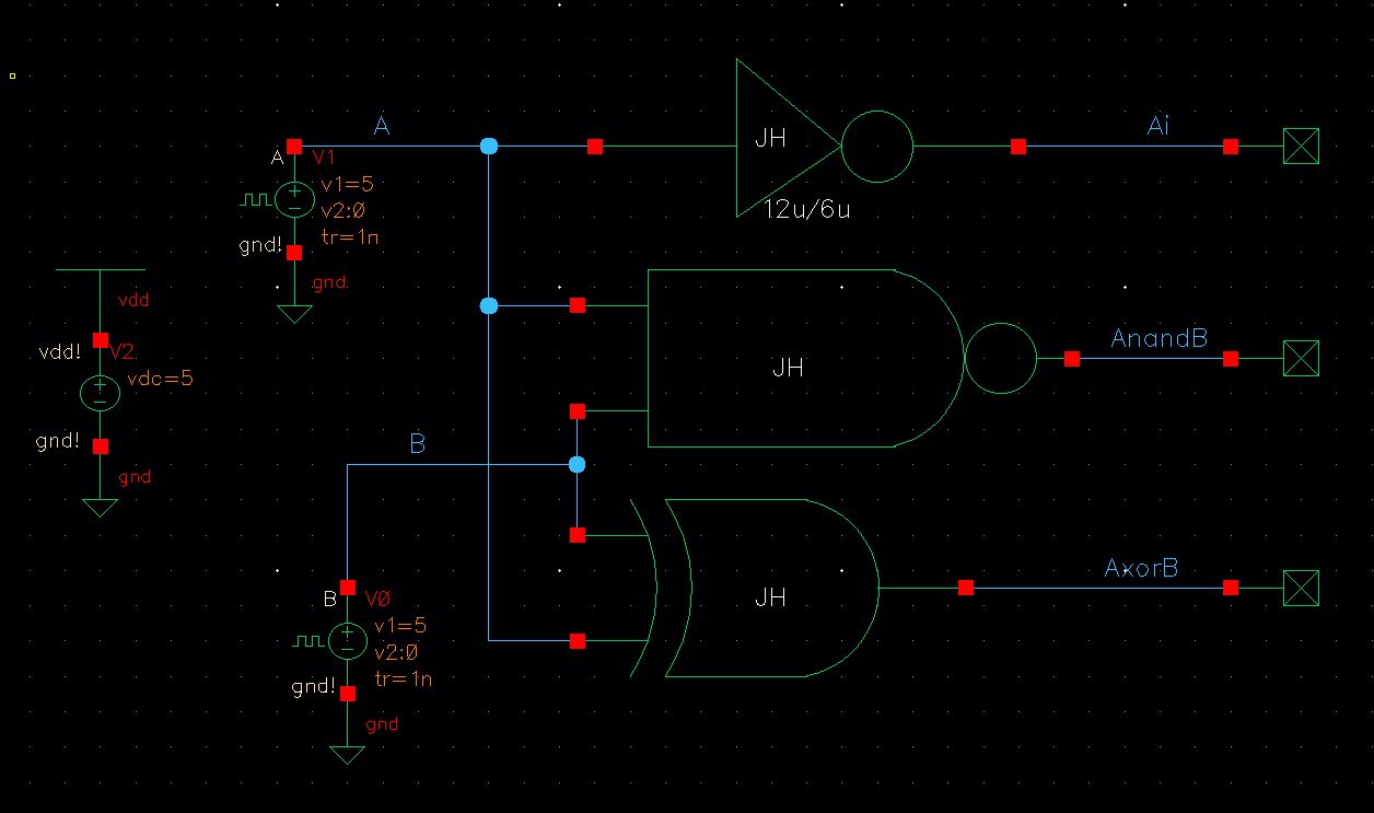
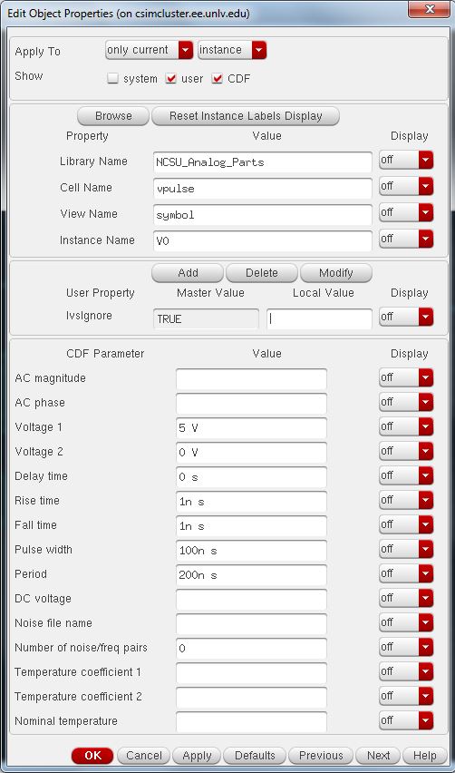
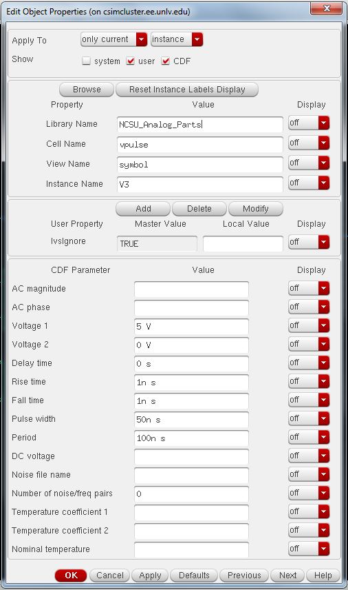
For our pulse sources, we are using the following for the A input source.
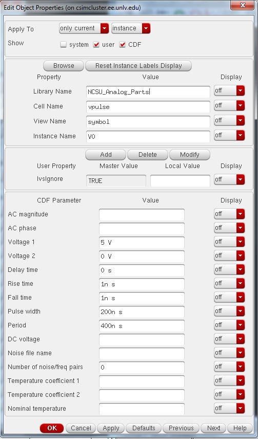
And we are using the following for the B input source. Notice how the pulse width and period is halfed of the A input source.
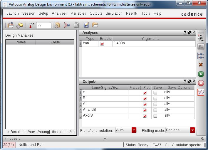
Now we can launch ADE L and use Spectre to sim this schematic. Making sure to plot all of the points below.
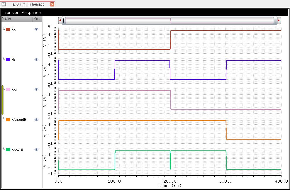
You will get the following graph when looking at each trace on a seperate graph.
Now we can create a full adder using the NAND and XOR gates.
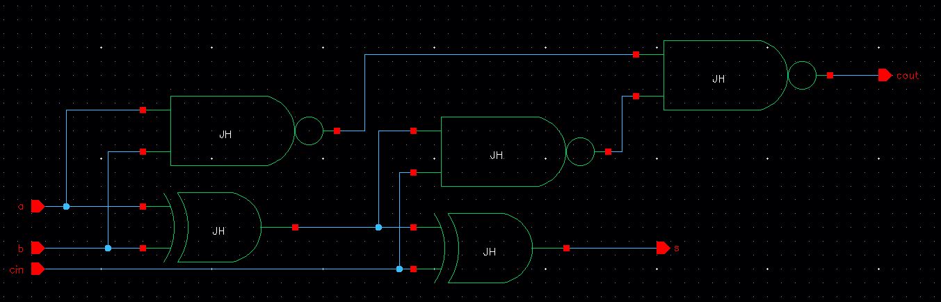
Full adder schematic using the symbols of the NAND and the XOR gates.
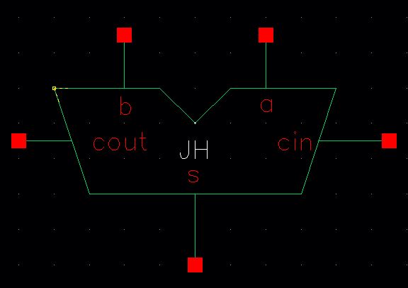
The symbol created for the full adder.
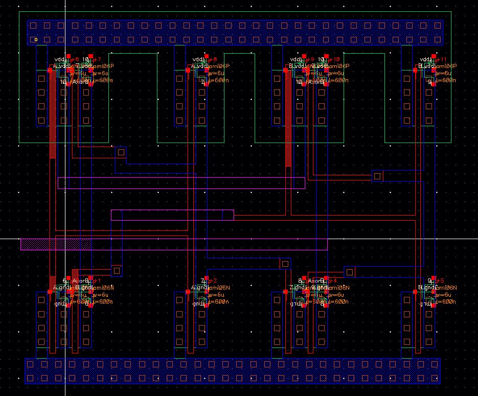
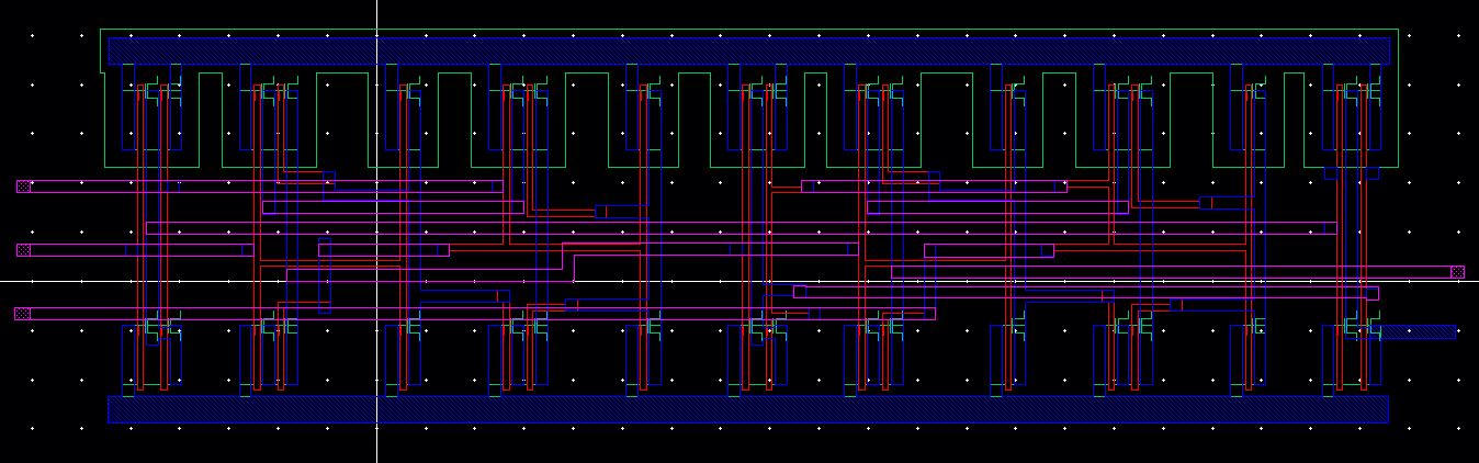
Moving on to the layout of the full adder. We used three NAND gates and two XOR gates.
Creating this layout was much more complicated. I instantiated the layout views of my NAND and my XOR gates.
Using
the flatten option in the Edit -> Heirarchy -> Flatten, I was
able to stretch the NAND gate and XOR gate enough to allow for more
connections for the adder.
I also connected the vdd! and the gnd! connections of the MOSFETS into a big row of ntaps and ptaps.
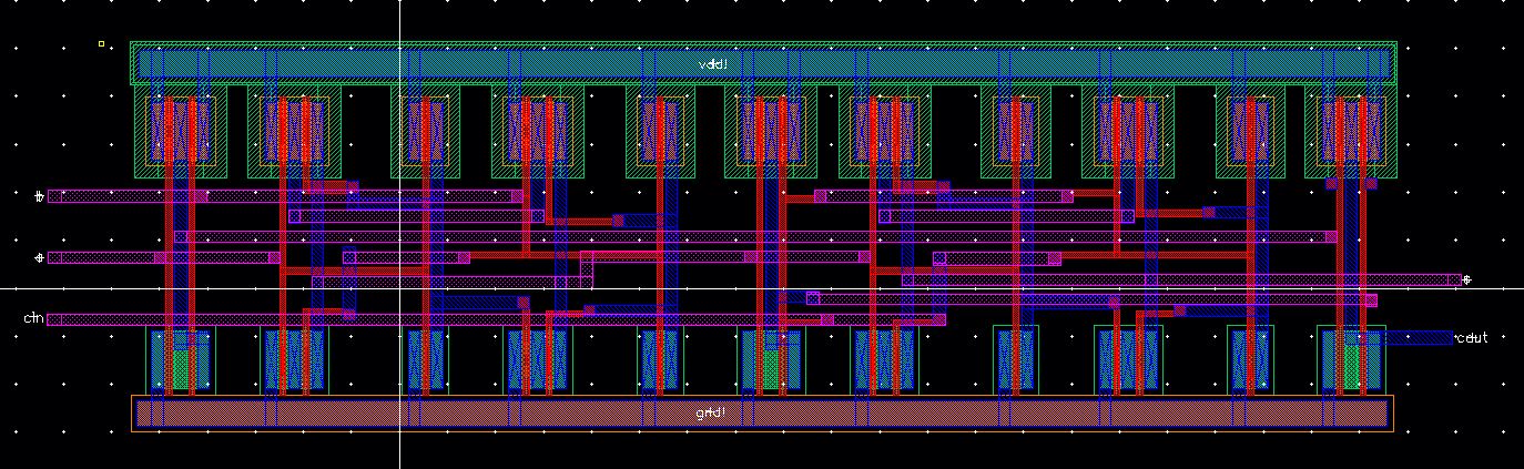
I made my input connections on the left of my adder as seen below.
I made my sum output and my cout on the right of my layout.
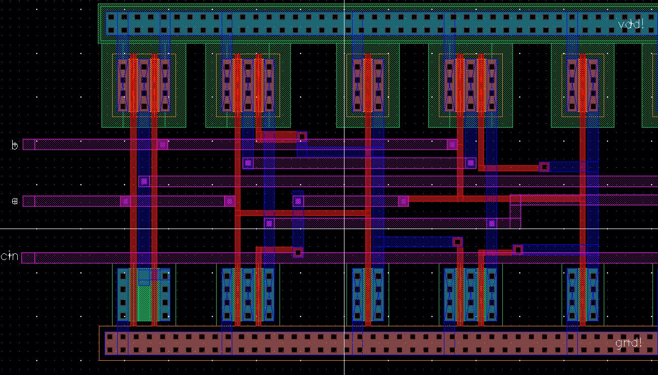
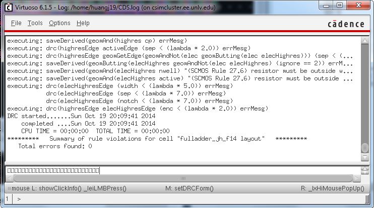
My layout passing DRC.
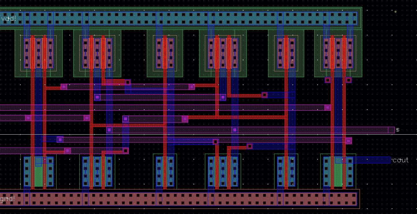
The extracted layout of full adder.
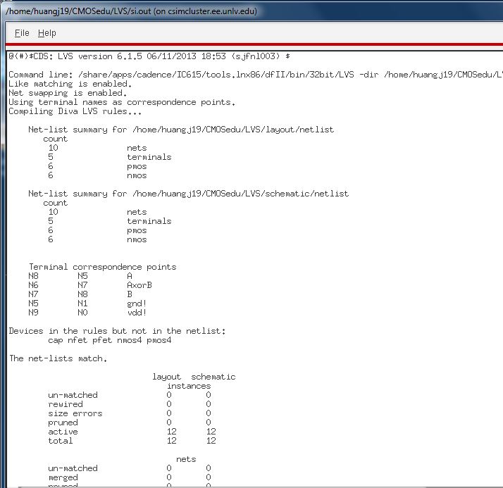
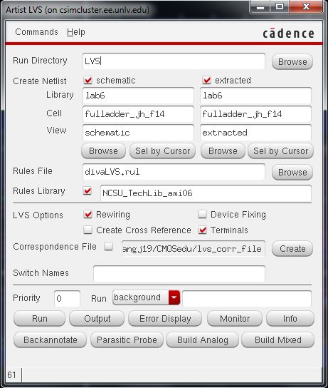
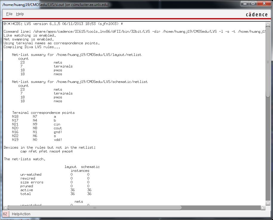
Now we can LVS the schematic and the extracted layout of the full adder.
Of course all the netlist match for the full adder.
Although I had a hard time trying to get this to work because of some connection mistakes.
I
was able to solve this by looking at the LVS Output and looking at
which nets were different, then going into my extracted view of my
layout and finding the nets that had errors and fixing them.
We can simulate the symbol we created for the full adder similiarly to how we simulate the NAND and the XOR gates.
We
create a schematic using the symbol and attaching the same A and B
pulse sources as previous and including the Cin pulse source.
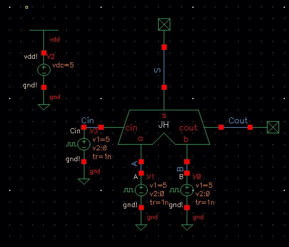
Notice that the pulse width and period is again half of the pulse source of B and a fourth of pulse source A.
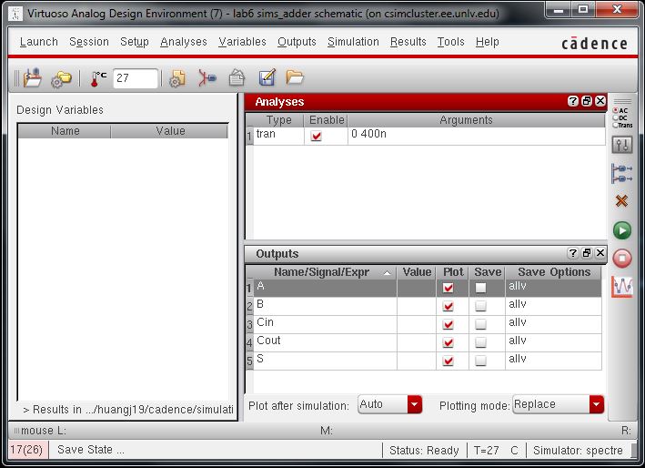
We can use ADE L and Spectre to simulate this full adder. Making sure to select all output variables seen below.
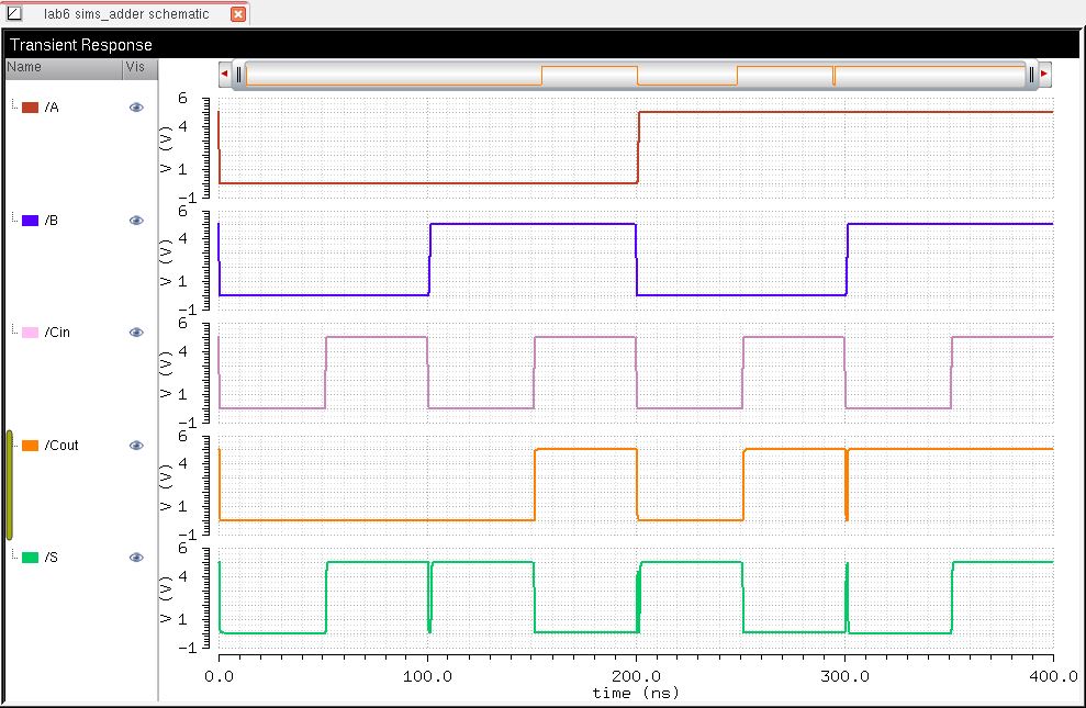
We should get the following graphs when we seperate each trace on it's own graph.
That will conclude our lab.
All the files from this lab can be found here.
Make sure to back up all your labs by zipping them up and sending them to yourself!

Return to EE 421L Labs