Make sure you check the update instances of your entire library.
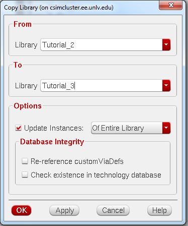
Now in the Tutorial_3 library, create a new schematic cell view called inverter.
Also open the schematic view of the NMOS_IV.
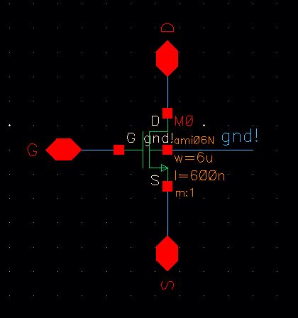
Copy the NMOS into your inverter window by copying the NMOS from the NMOS_IV window and dragging it over to the inverter window.
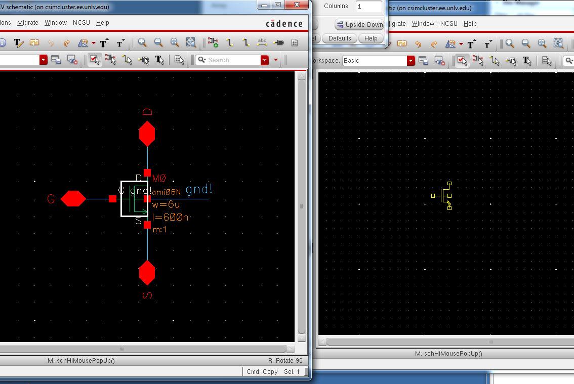
Now close the NMOS_IV window and open the PMOS_IV window and copy it over to the inverter window again.
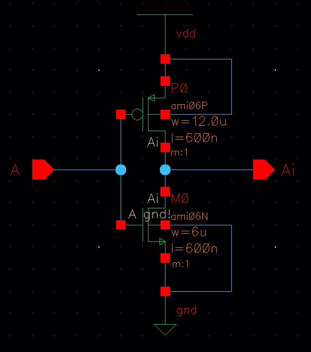
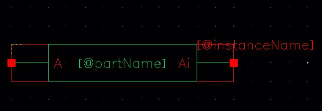
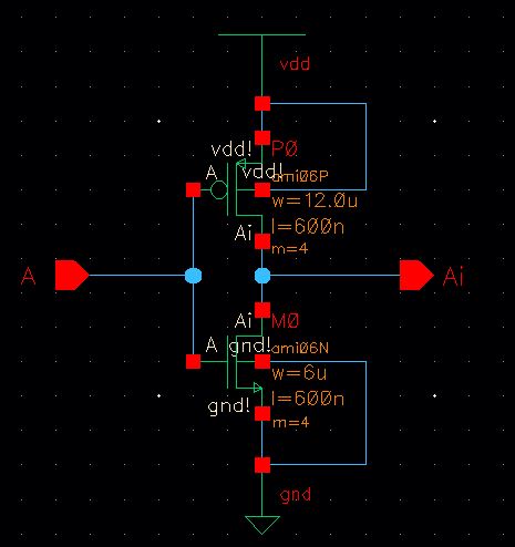
Now instantiate vdd and gnd supply nets and add the pins A(input) and Ai(output) seen below.
Now check and save.
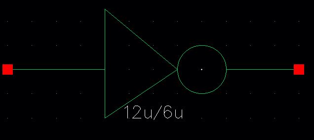
Create a symbol from this schematic.
Click OK for the pin selections.
You should get the following below.
Delete everything in the inverter symbol except for the pins.
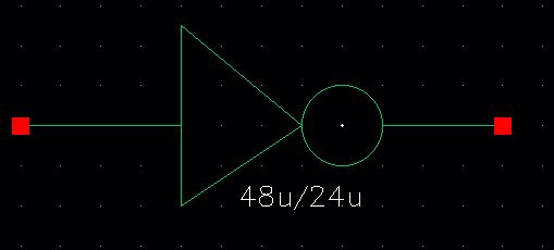
Draw the inverter symbol seen below by using the create -> shape -> line/circle.
Make sure your pins are in the correct order, A is an input and AI is the output.
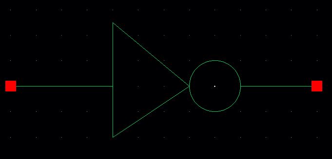
Check and save the symbol.
Now lets create a layout view for the inverter.
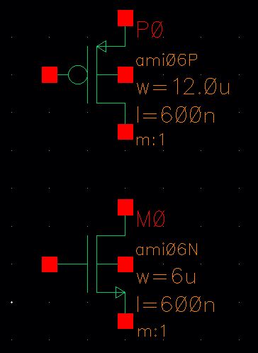
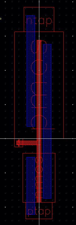
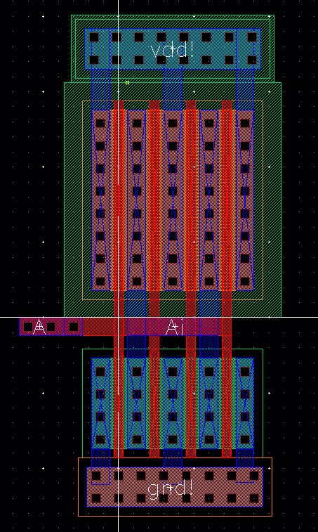
Instantiate the following cells seen below, which is a nmos (6u/0.6u), pmos(12u/0.6u), ntap, ptap, and m1_poly.
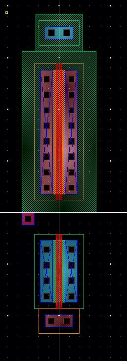
Now add rectangles on poly and metal 1 as seen below.
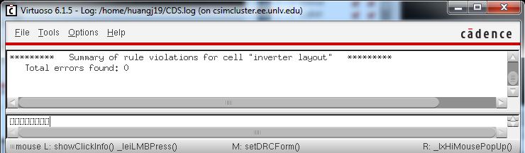
DRC and save your layout.
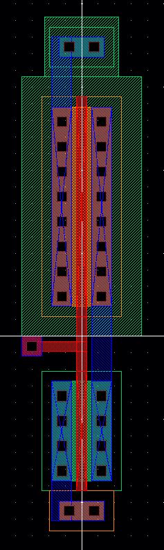
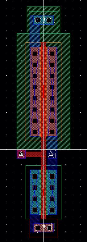
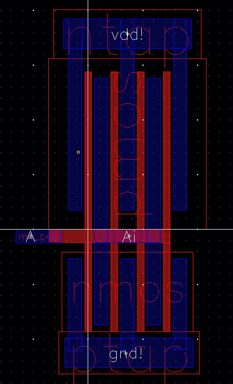
Just to check, change your display levels and you should have the following.
Now let's add pins on metal1 for gnd! and vdd! (InputOutput), A (input) and Ai (output).
DRC and save your layout.
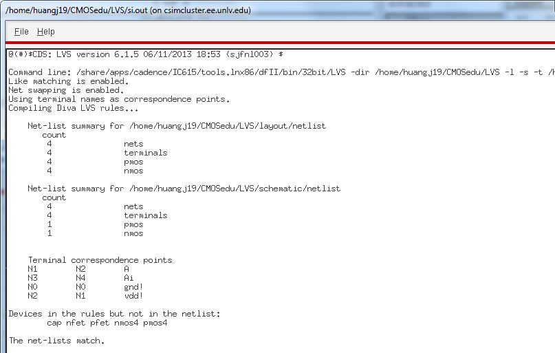
Extract your layout.
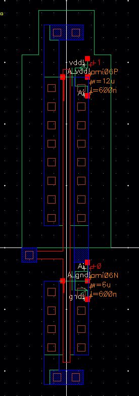
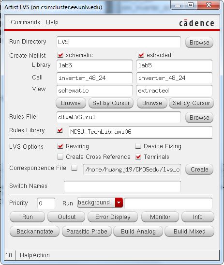
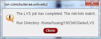
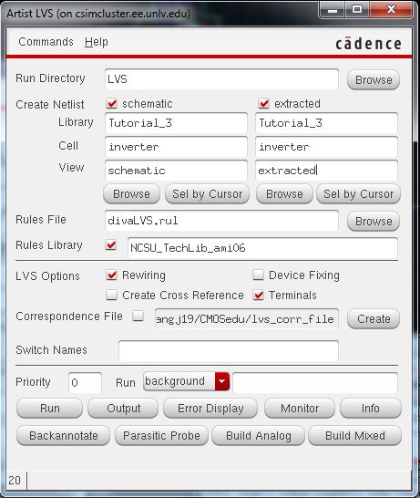
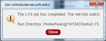
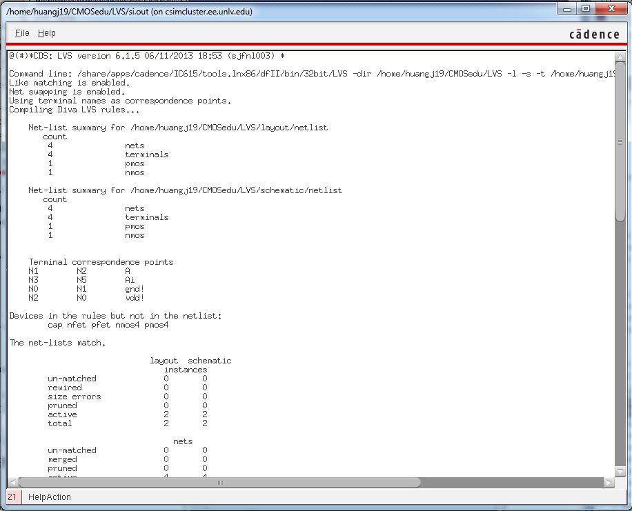
LVS your extracted with your inverter schematic.
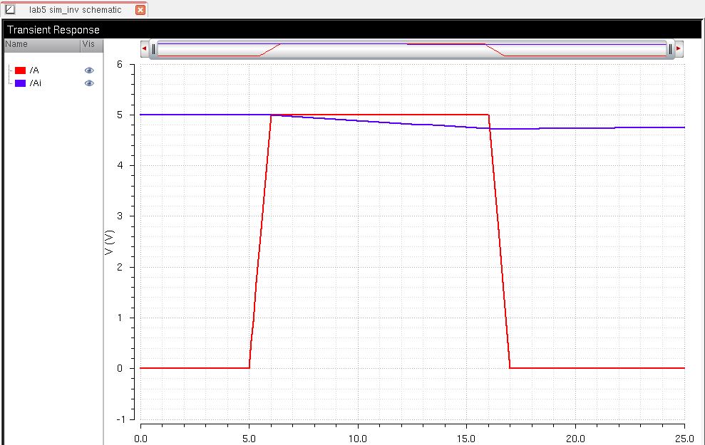
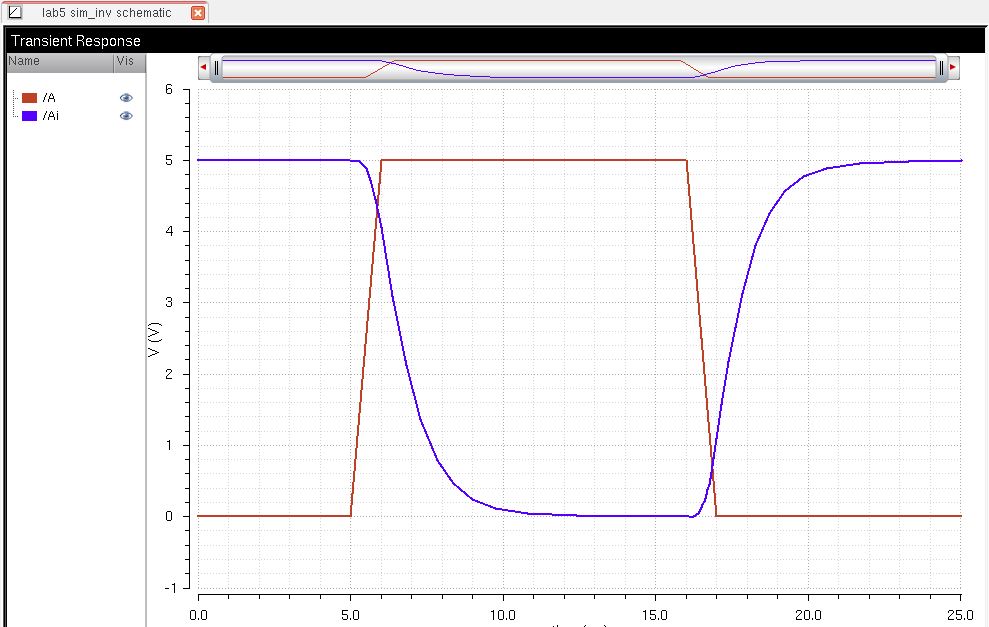
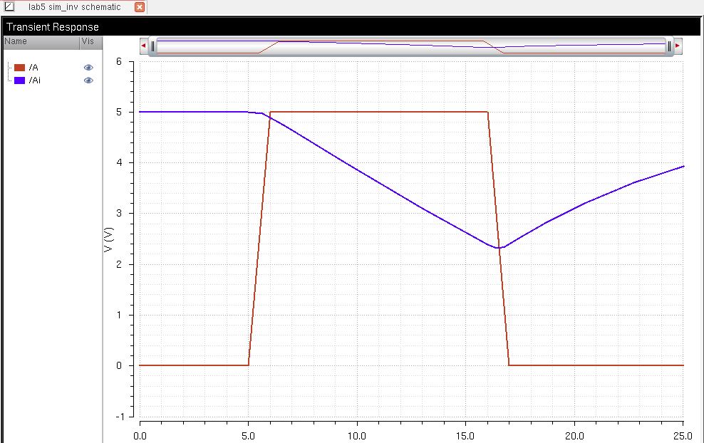
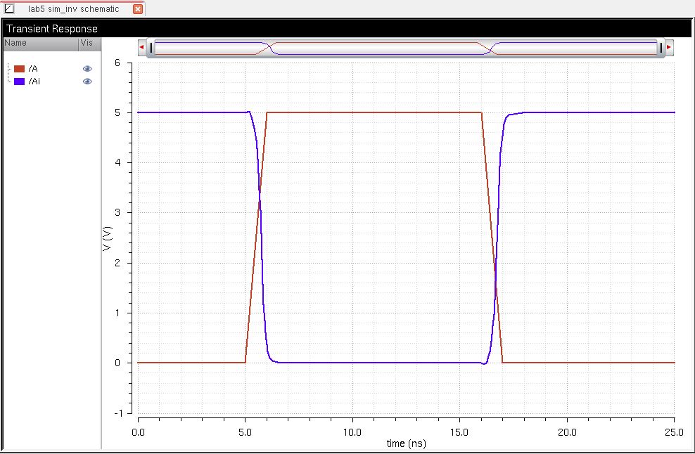
Now let's simulate the inverter.
Create a schematic cell view called sim_inverter_dc.
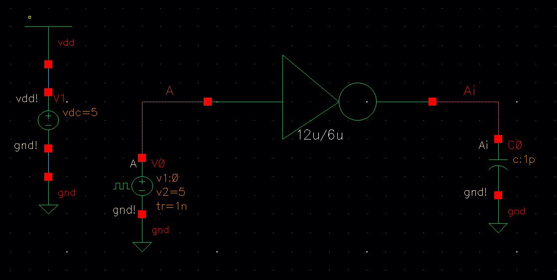
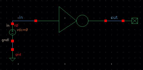
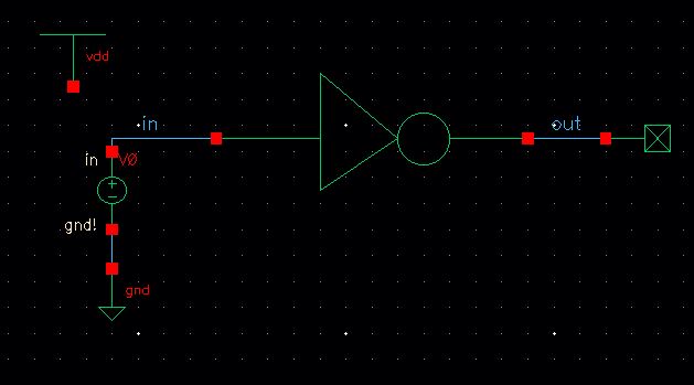
Draw the following schematic seen below, the symbol on the right is the no-connection symbol (basic library, Misc -> noConn), this will help us from getting an error on the floating point.
Now launch ADE L and select the correct models, in this case, you need the ami06P.m and ami06N.m models.
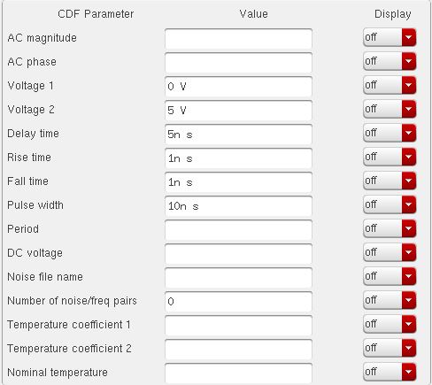
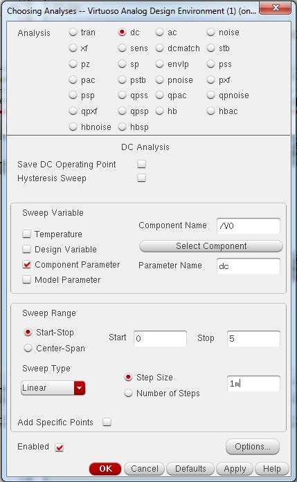
Select a dc analyses with the following values.
Select your in and out wire to be your outputs to be plotted.
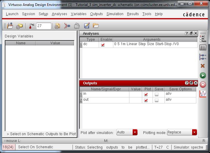
Save the state in cell view and run the dc analyses.
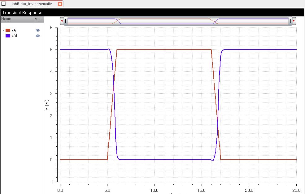
Right click split current strip and click trace and you should get the following get the following graph.
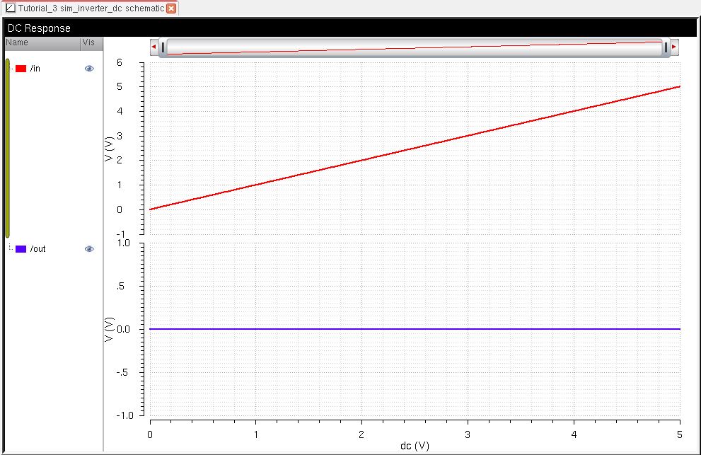
Note that the output is zero, this is because we didn't specify our vdd!
Let's add a vdd! and see what happens.
Add vdd! into our schematic.
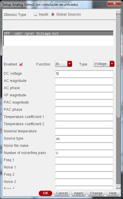
Go back to yoru ADE and go to setup -> stimuli and set the parammeters seen below. make sure you hit Apply when you are done.
Save the state and run the simulation.
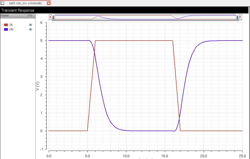
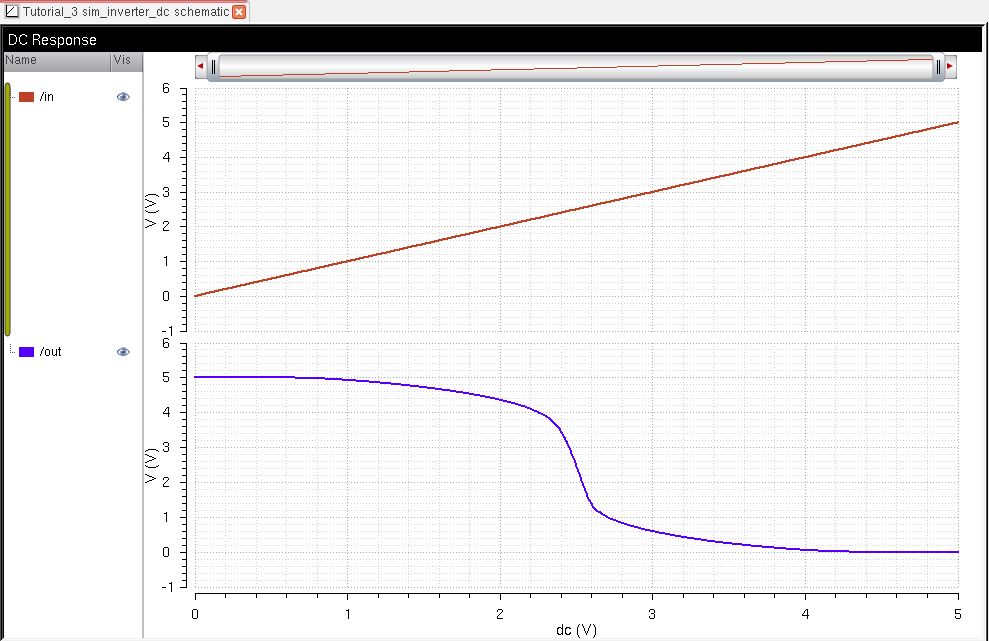
Now you should get the following graph.
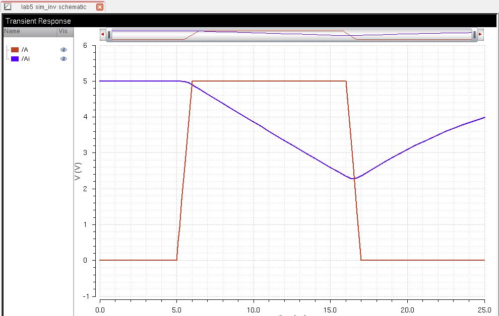
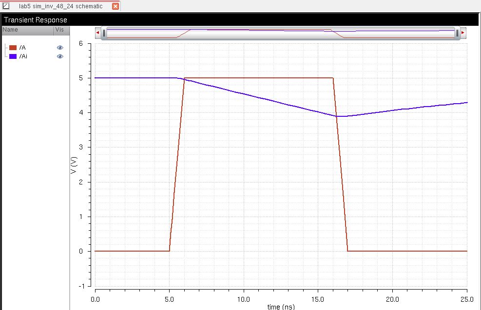
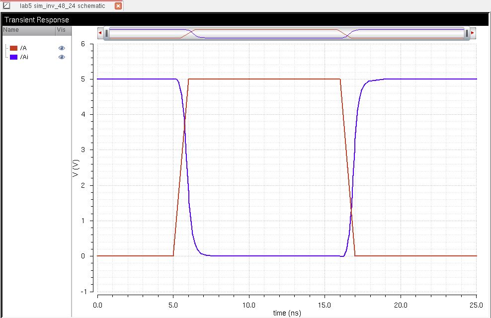
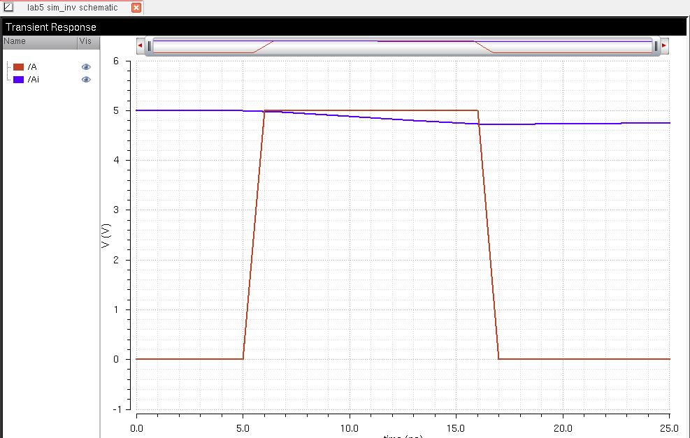
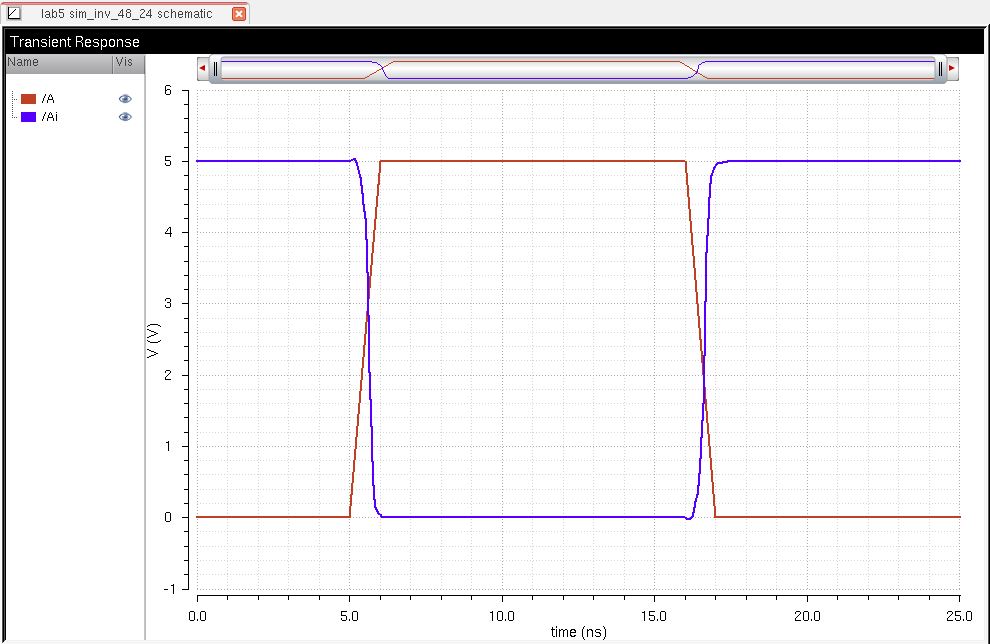
Now let's simulate the extracted layout.
Setup -> Environment and add extracted in front of the schematic.
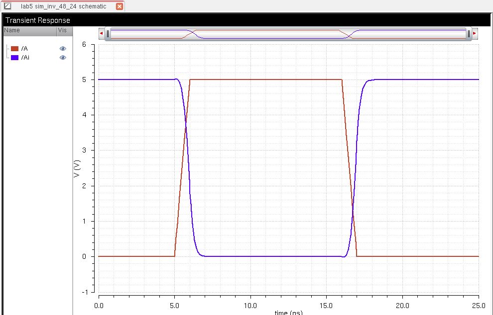
You should get the same graph.
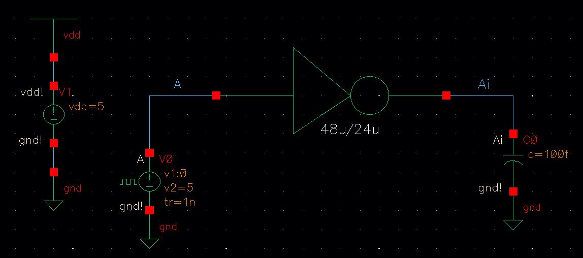
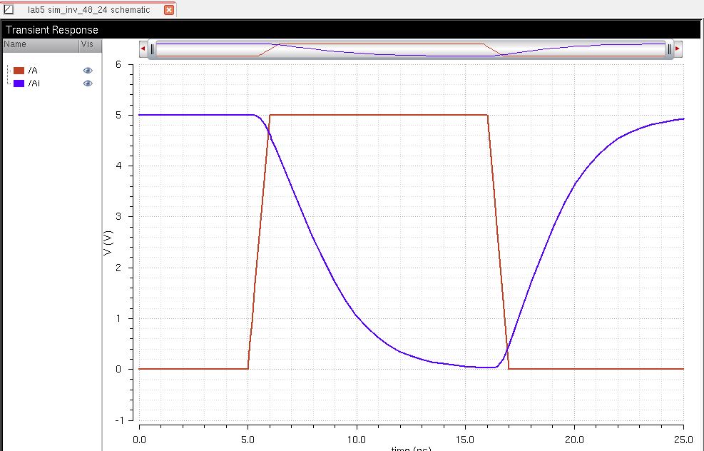
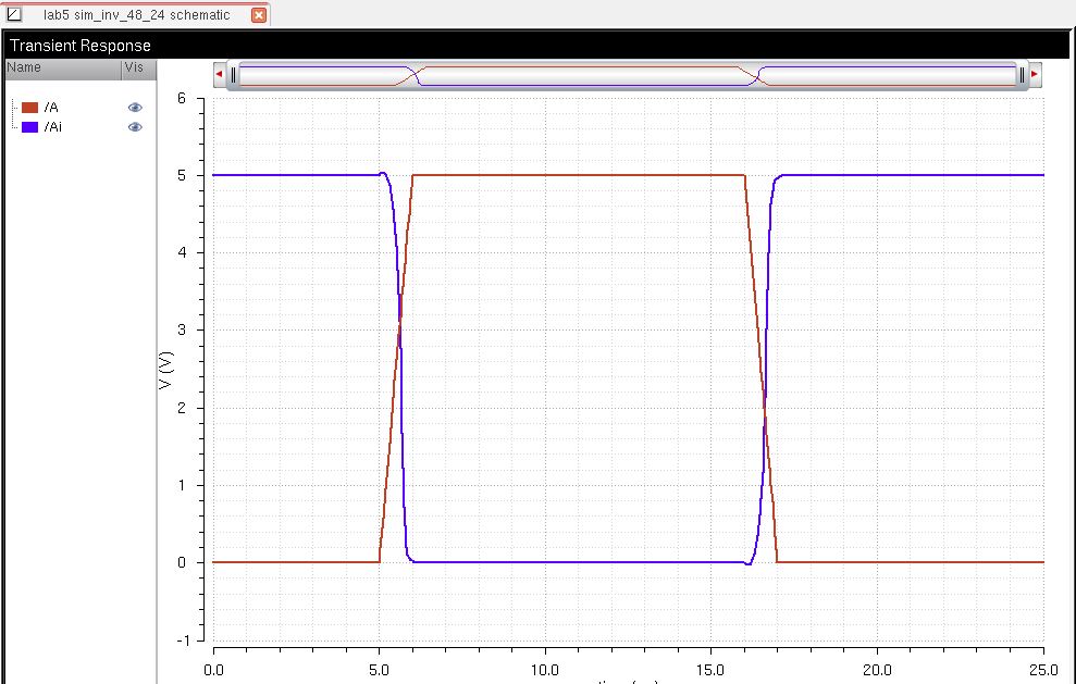
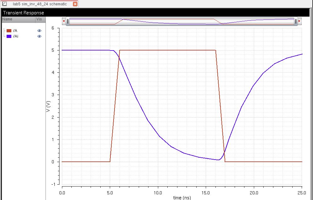
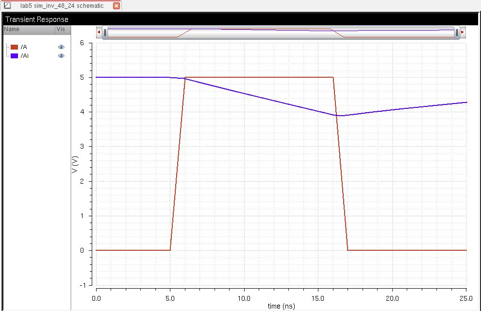
Let's now create a 48u/24u inverter.
Copy over your 12u/6u inverter cell view into inverter_48u_24u.
Open the schematic view and edit the properties of your NMOS and PMOS.
Change the multiplier value to 4 for both.
Now create a symbol from your cellview.
Delete everything in the cell and redraw the inverter symbol previously.
We labeled the inverter 48u/24u to differentiate it from the 12u/6u inverter.
We can go back to the symbol view and label the 12u/6u inverter.
Check and save your inverters and close out of them.
Open your copied layout of your 12u/6u inverter.
Change the multiplier to 4 for your NMOS and PMOS layout.
You should also increase the size of your ntaps and ptaps at this point.
Make the connections similiar to how you made your 12u/6u inverter.
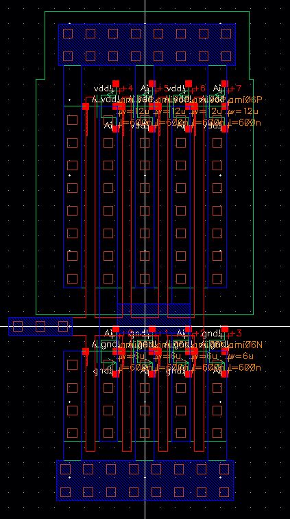
It should look similiar to the image below.
Your connections for each pin should look like below.
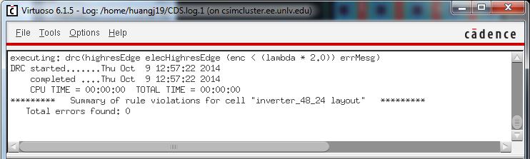
DRC your layout and ensure there are no errors.