Lab 4 - ECE 421L
Authored
by John Huang.
Huangj19@unlv.nevada.edu
October 4, 2014
In
this lab you will learn how to layout a NMOS and a PMOS. You will also
learn how to the gate, source and drain of a NMOS and PMOS are related
to their respective drain current.
First copy your Tutorial_1 folder into a new library called Tutorial_2 by right clicking and clicking copy.
Make sure you select Update Instances so that your cells of Tutorial_2 will not reference your Tutorial_1.
Now create a new cell view in Tutorial_2 called NMOS_IV_3. This indicate we'll use a 3 terminal transistor.
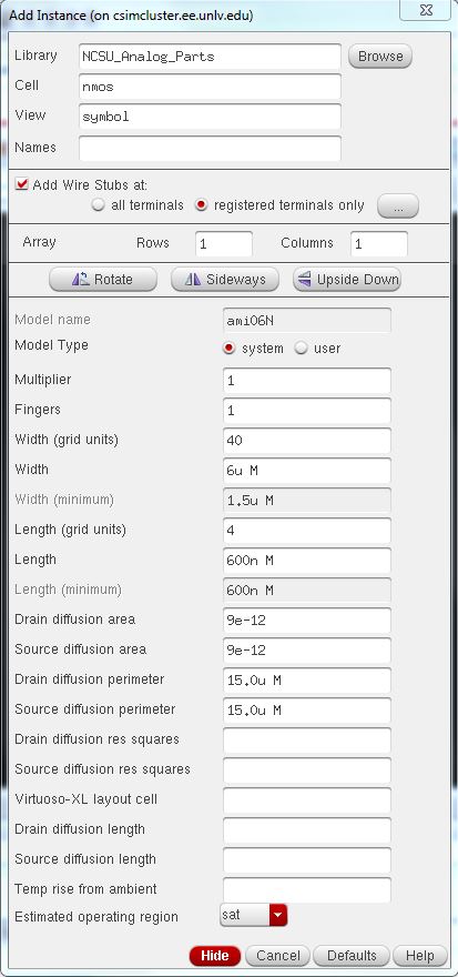
Create an instance from the NCSU_Analog_Parts library and in the N_transistors then selecting an nmos.
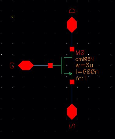
Set the transistors width to 6u and length at 600 nm and place it in your schematic.
Next add pins with the direction of InputOutput and wires similiar to below.
If you want to move your pins you can use the stretch tool (bindkey s), this object will stay attached to the wire or anything that is not selected.
Now let's create a symbol view for this schematic.
Go to Create -> Cell View -> From Cell View
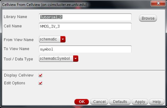
Press OK then OK again, the pin location does not matter.
Now delete everything in the cell except the pins.
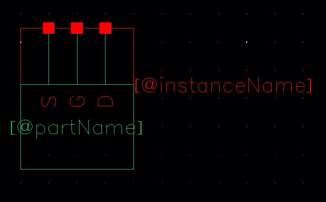
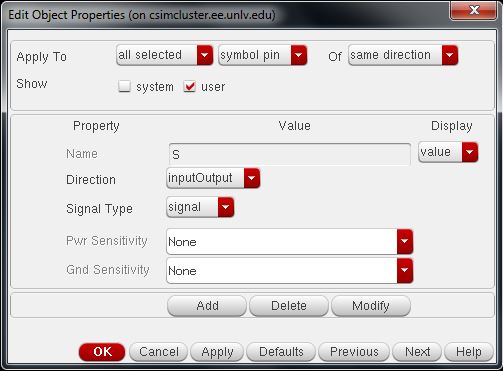
Now select all the pins and edit their properties (q).
Use the drop down menu and select 'all selected' and change the Display to 'value'.
Continue
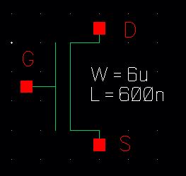
by drawing a MOSFET symbol and moving the pins similiar to the picture
seen below. Add text by using Create -> Note -> Text
When finished check and save your symbol.
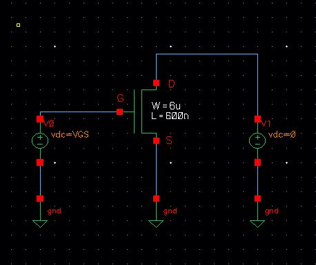
Now lets go back to the Library Manager and create a new cell view called sim_NMOS_IV_3.
Instantiate the NMOS_IV_3 you just created and create the schematic below.
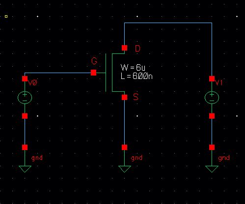
Now make the V0 voltage to VGS and your V1 voltage to 0 as seen below. Check and save the schematic.
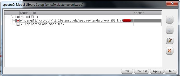
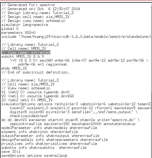
Now
launch ADE. Go to Setup -> Model Library and add (clicking the
browse button that has '...' on it) the ami06N.m from the
/$HOME/ncsu-cdk-1.6.0.beta/models/spectre/standalone.
For a PMOS use the ami06P.m.
Go
to Variables -> Edit and add VGS as the name and 0 for the value. It
will show up in the design variables window in the ADE window.
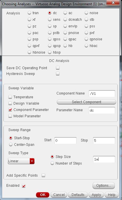
Now set up a dc sweep seen below.
Select the D Pin on outputs to be plotted and ensure that both plotted and save are selected.
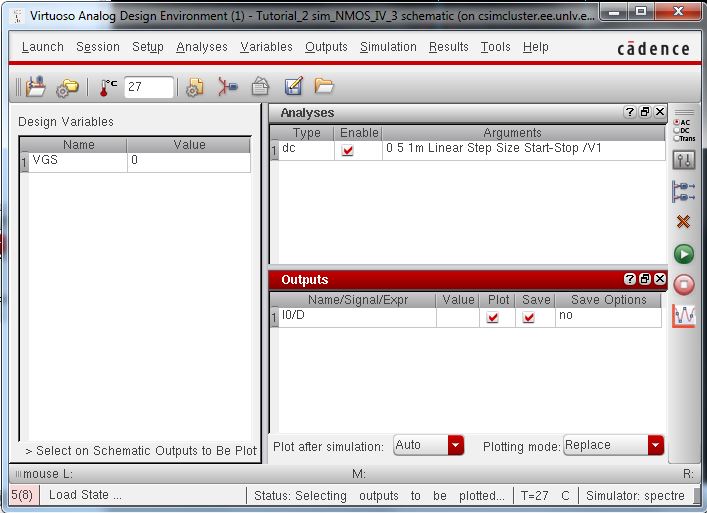
Save the simulation state as a cellview.
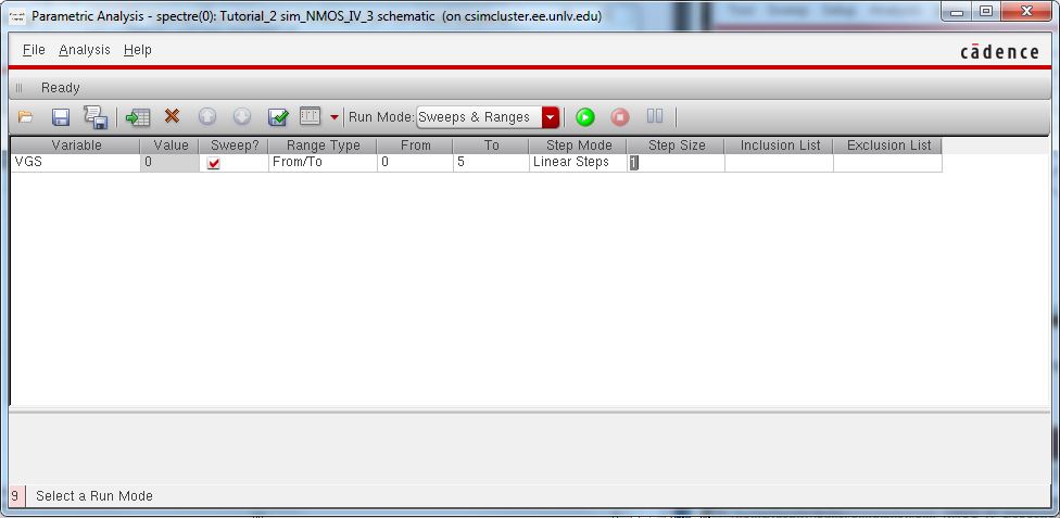
Now go back to ADE and choose Tools -> Parametic Analysis and set the parameters seen below.
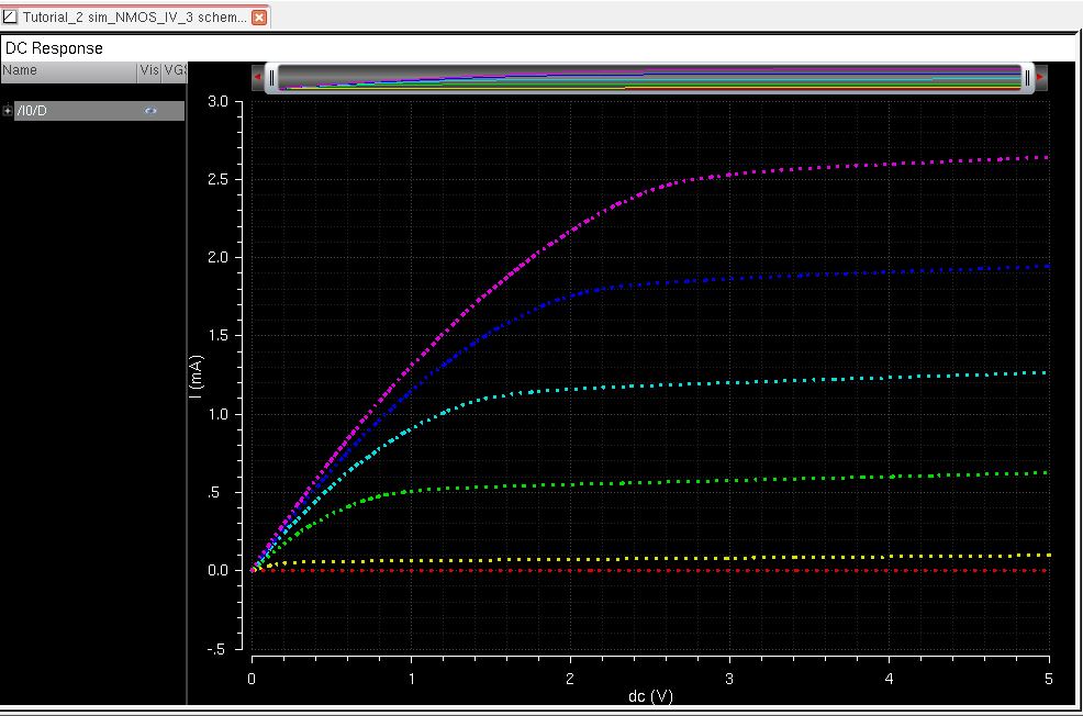
Now click the green play button to see the MOSFET IV curves below.
Save the state and close the schematic of sim_NMOS_IV_3.
We can now start the layout this cell and simulate it.
Create a layout view for the NMOS_IV_3.
Make sure the gravity is off in the Layout Editor Options.
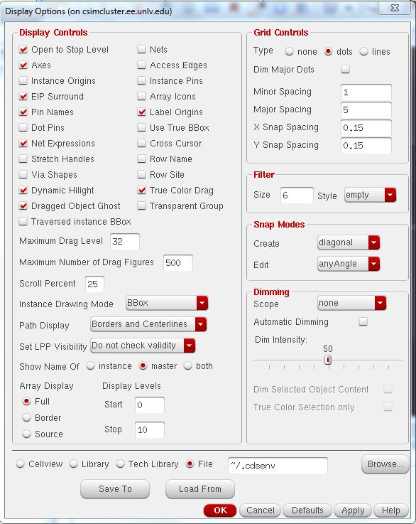
And make sure that the Display Options are the
same as the image below. We are saving these options when we select
Save To so that everything we open a layout it will default to these
settings.
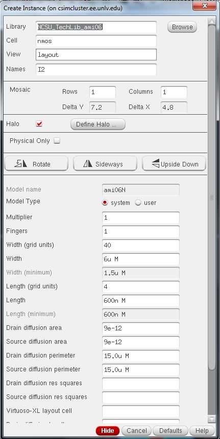
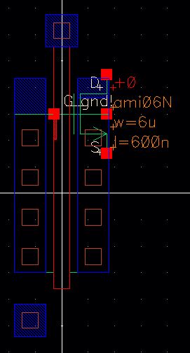
Next we instantiate an nmos device that will be 6um wide and 600 nm long.
Next add a ptap cell so that it will look like the following below.
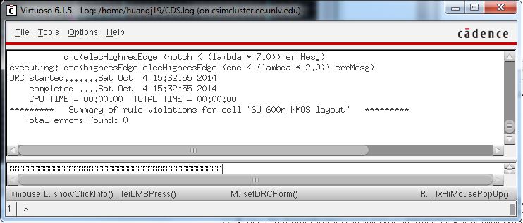
DRC the layout to make sure there are no errors.
Now
add rectangles of metal1 to connect the source to the p-substrate and
to the drain. Also instantiate a m1_poly and a poly rectangle to
connect the gate to the m1_poly.
DRC the layout once again.
Now add D, G, and S InputOutput pins on metal1 as seen below.
DRC the layout once again and save the cell view.
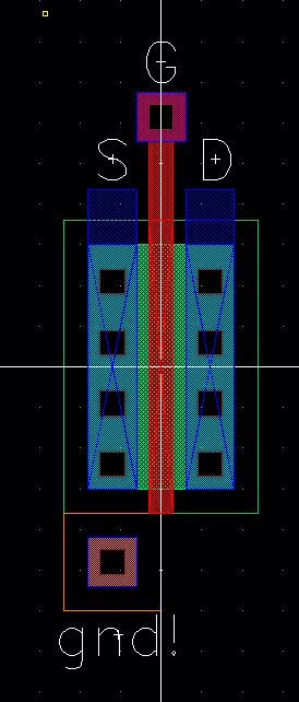
Extra the layout and open the extracted cell view.
We
can see the the symbol displays 4 terminals, not 3 compared to the
transistor we used in the schematic, this is because we assume the the
p-substrate is tied to gnd!
Continue by running a LVS as seen below.
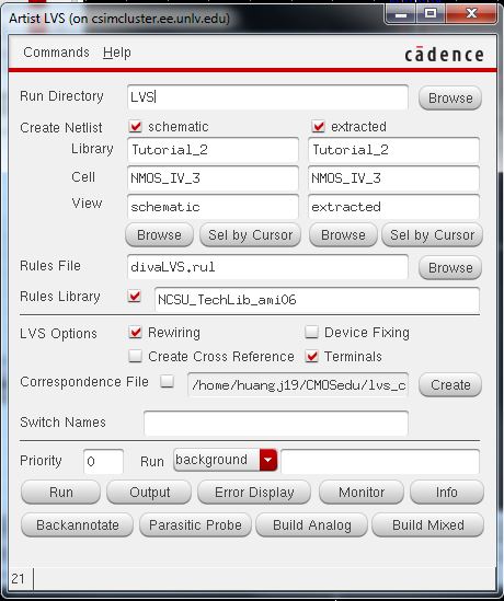
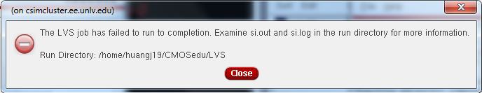
We will see that the job has failed, click OK.
Go to the Artist LVS window and click Info and Log File.
Scrolling down we will see the *Error*.
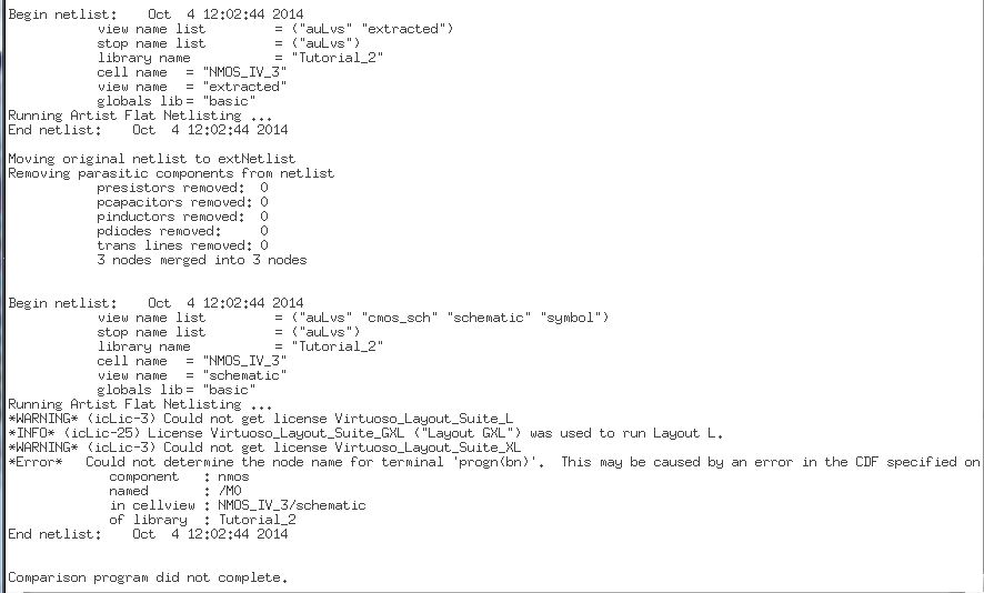
The
error is related to the bulk (p-substrate) connection for the NMOS,
this connection is tied to gnd! for a NMOS and vdd! for a PMOS.
We now have to modify the layout.
Delete the metal1 rectangle and pin connecting the S Pin to the bulk (ptap).
Next add metal1 rectangles over the S and B metal.
Add pins as seen below.
DRC your layout and save it.
Extract your layout and open your extracted file.
You can see that the NMOS is now connected the gnd!
Run LVS again with the new extracted layout.
Again we will fail the LVS and when checking errors in the log file it will give us the same error.
Now we can try to use a 4-terminal transistor in our schematic to run LVS.
To do this, we must first close all our cell views and rename the NMOS_IV_3 cell to NMOS_IV and the sim_NMOS_IV_3 to sim_NMOS_IV
Open
the schematic view of NMOS_IV and change the NMOS symbol as seen below
by selecting the NMOS and changing its cell name to nmos4.
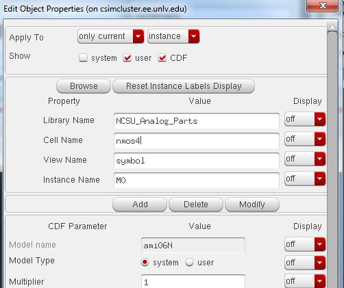
Move the symbol to connect to the correct wires and add a new wire label gnd! to the new terminal.
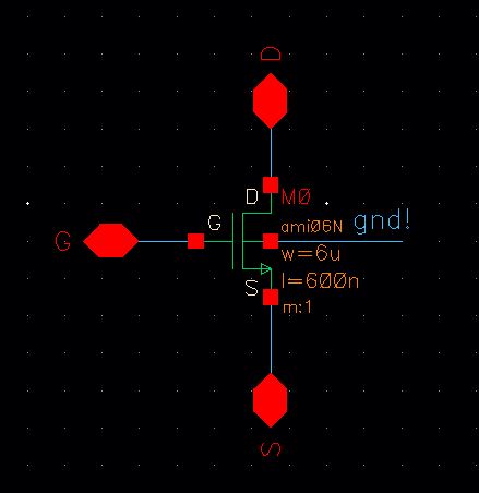
Save the schematic.
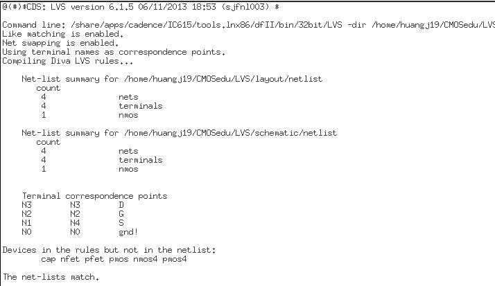
Open the extracted view and perform a LVS with the new schematic.
Now your LVS will pass and your net-list will match.
Now lets simulate the extracted layout.
Open the schematic view of the sim_NMOS_IV and launch ADE L.
Load the state from cell view.
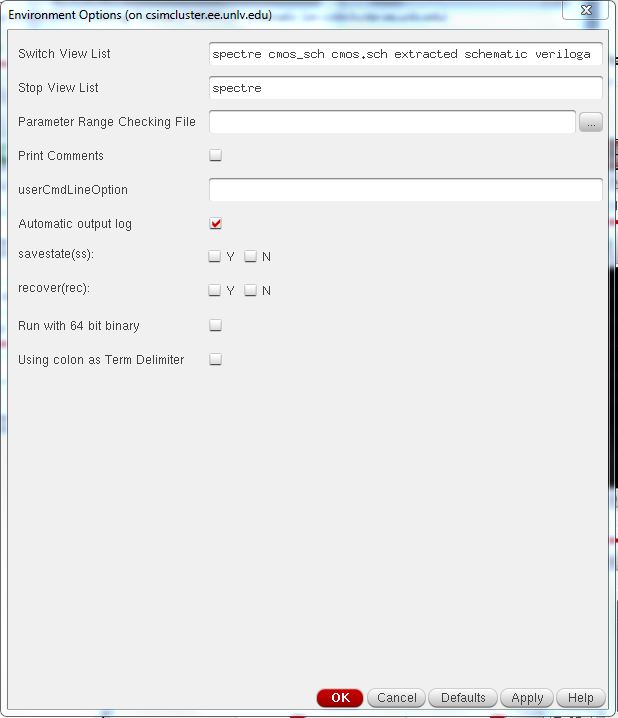
Go
to Setup -> Environment and enter extracted before schematic. This
is so that the extracted view is sused before the schematic when
running the sim.
Now run a parametric analysis again with the same values as before and you should get the same graph.
To
ensure that we are simulating the extracted view and not the schematic
view go back to your ADE window and go to Simulation -> Netlist
-> Display and you will seethat the View name is extracted.
Now we can repeat these steps for a PMOS device, but in a concise manner.
Create a schematic cell view called PMOS_IV.
Instantiate a 4 pin pmos and make the width 12u and length 600n.
Add the InputOutput pins as seen below.
Check and save the schematic.
Now lets create a symbol for the schematic.
Check and save the symbol.
Now let's crate the layout.
We will be using a pmos cell and a ntap as seen below.
DRC and save the layout.
Now extract the layout and open the extracted view.
Save and close all open cell views.
Now create a new cell called sim_PMOS_IV and draft the following schematic.
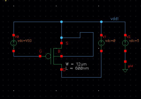
Check and save.
Launch ADE and go to Setup -> Model Libraries and select the PMOS models for AMI06.
Variables -> Edit and add VSG with a value of 0.
Next select the outputs and the source terminal of the transistor, having both Plot and Save selected.
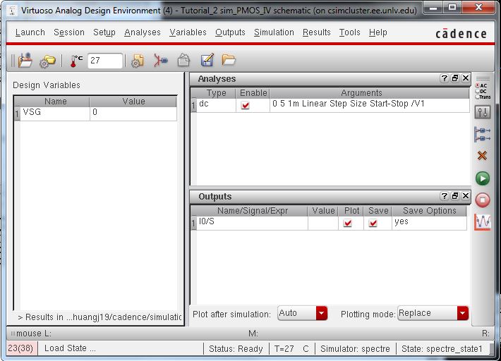
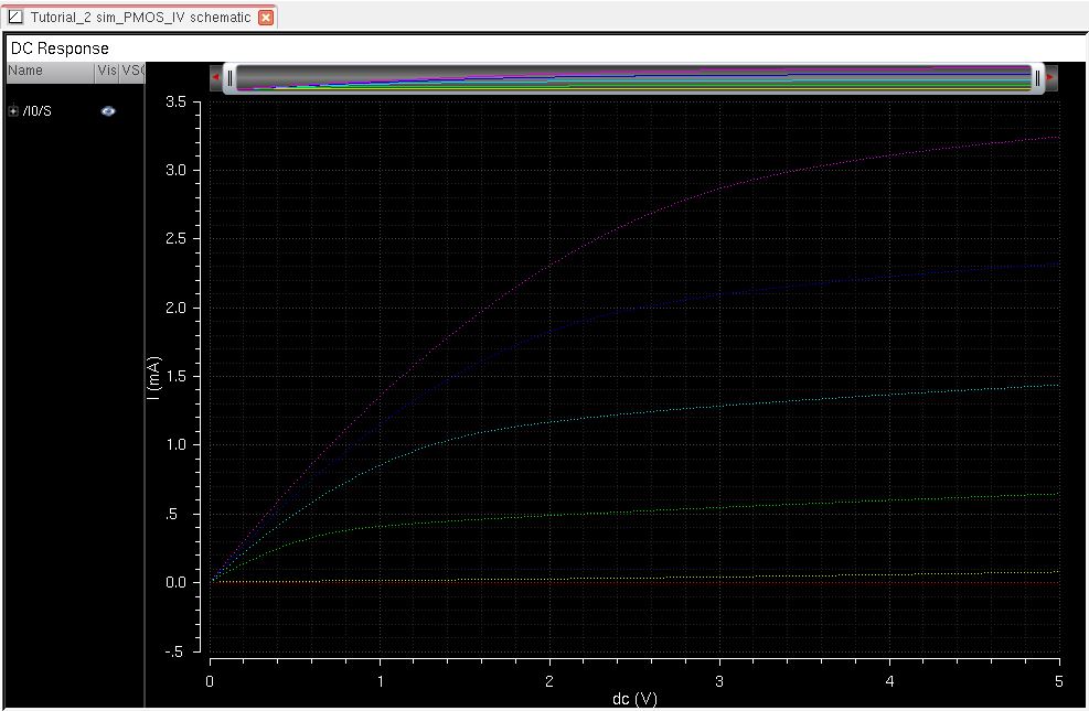
Now run the parametric analysis the same as before but changing your variable to VSG.
You should get the following graph.
Now lets simulate the extracted layout.
In the ADE go to Setup -> Environment and added extracted before schematic.
Run the parametric analysis again and you should get the same results.
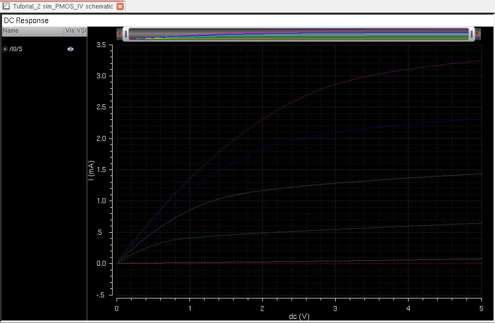
Verify again that we are using the extracted view name in the netlist.
Now we have sucessfully created a symbol and a layout of a NMOS and a PMOS!
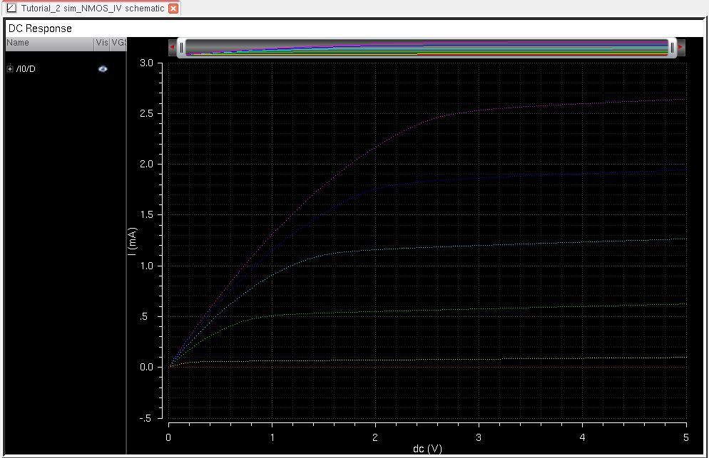
We can now take a look at some NMOS relations.
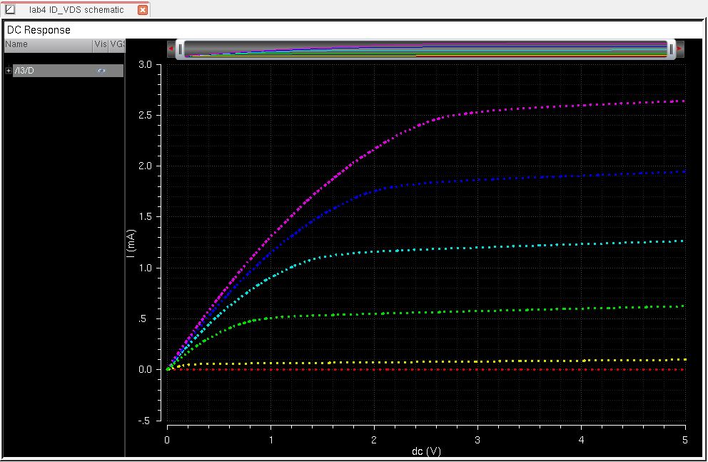
First let's take a look at the
curve of ID versus VDS of an 6u/600n w/l NMOS device when the VGS
varries from 0 to 5 V in 1 V steps, and when VDS varies from 0 to 5 V
in 1mV steps.
Create a schematic cell view in your lab4 library, name it ID_VDS.
Draw the following schematic seen below, we are using the NMOS we created previously. 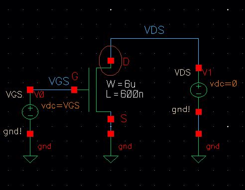
Check and save your schematic.
Now open ADE L.
Make sure you choose your model library in the ami06 as the NMOS.
Create a dc response according to the type of respons we noted above.
Create a design variable name VGS and set the value to 0.
Make sure you select your Output variable as your Drain pin.
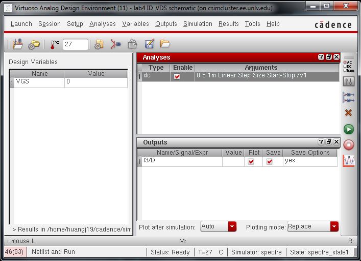
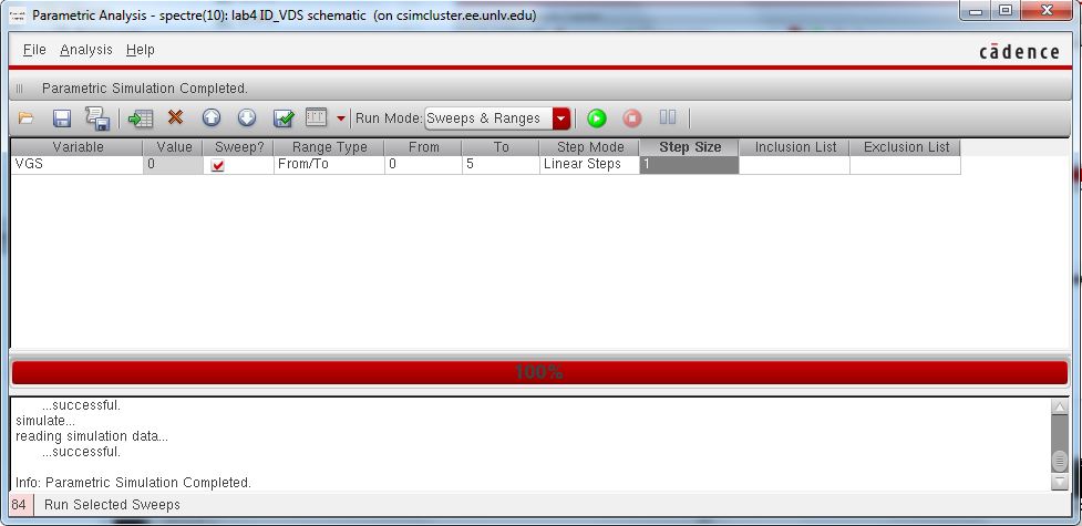
Go to Tools and Parametric Analysis again.
Set up your values seen below and run the analysis.
We should get the following graph.
Secondly let's take a look at the curve of ID versus VGS of an 6u/600n w/l NMOS
device when the VGS varries from 0 to 2 V in 1 mV steps, and when VDS is 100 mV.
Create a schematic cell view in your lab4 library, name it ID_VGS.
Draw the following schematic seen below, we are using the NMOS we created previously.
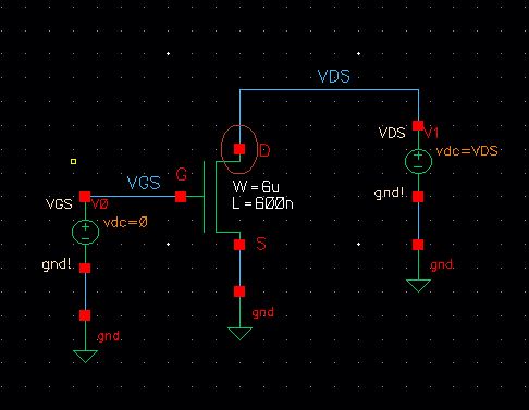
Check and save your schematic.
Now open ADE L.
Make sure you choose your model library in the ami06 as the NMOS.
Create a dc response according to the type of response we noted above.
Create a design variable name VDS and set the value to 0.
Make sure you select your Output variable as your Drain pin.
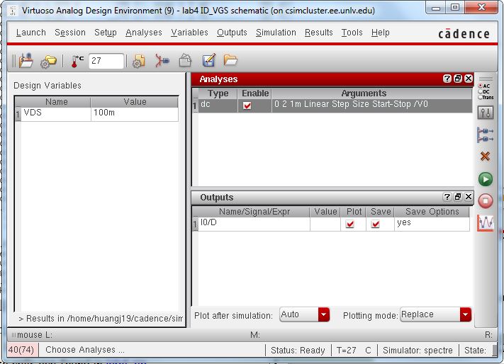
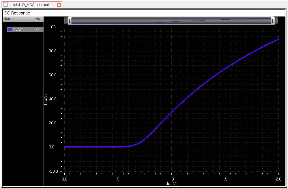
Run the dc response and we should get the following graph.
We can now look at some PMOS relations.
First
let's take a look at the curve of ID versus VSD of an 12u/600n w/l PMOS
device when the VSG varries from 0 to 5 V in 1 V steps, and when
VSD varies from 0 to 5 V in 1mV steps.
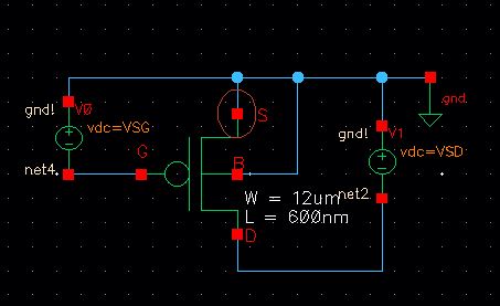
Create a schematic cell view in your lab4 library, name it ID_VSD.
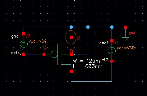
Draw the following schematic seen below, we are using the PMOS we created previously.
Check and save your schematic.
Now open ADE L.
Make sure you choose your model library in the ami06 as the PMOS.
Create a dc response according to the type of response we noted above.
Create a design variable name VSD and VSG and set both of their values to 0.
Make sure you select your Output variable as your Source pin.
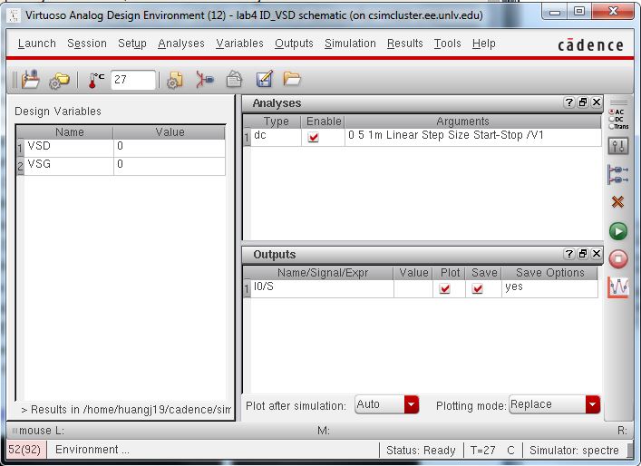
Go to Tools and Parametric Analysis again.
Set up your values seen below and run the analysis.
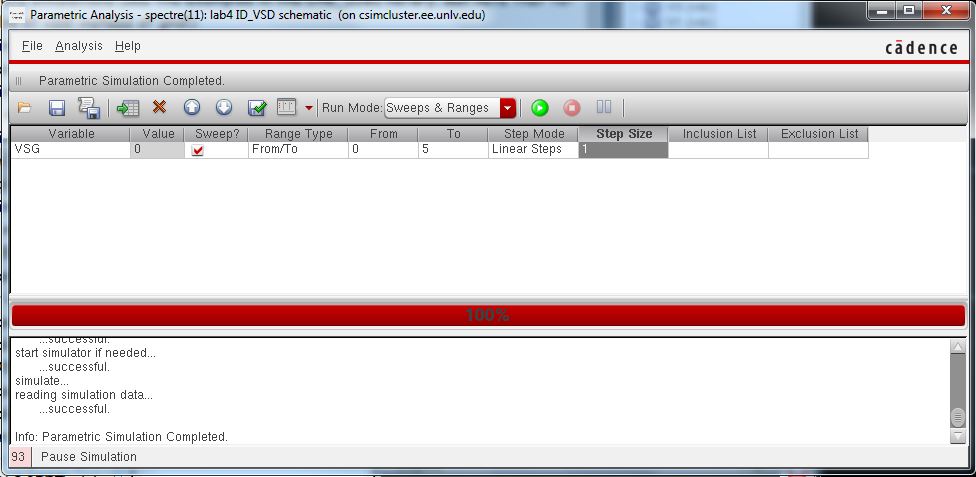
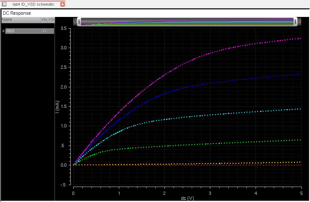
You should get the following graph below.
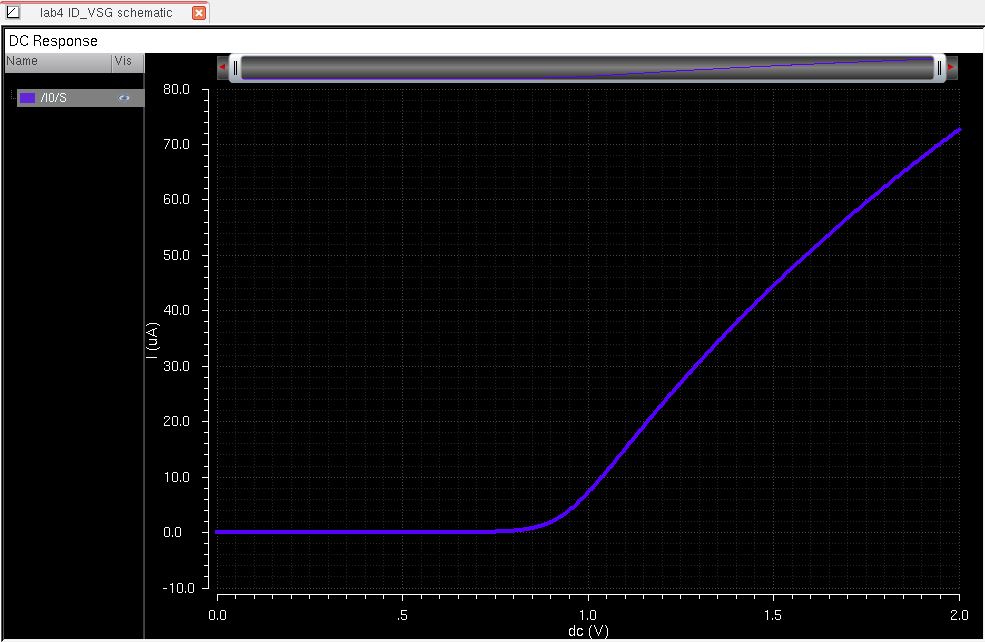
Secondly let's take a look at the curve of ID versus VSG of an 12u/600n w/l PMOS
device when the VSG varries from 0 to 2 V in 1 mV steps, and when VSD is 100 mV.
Create a schematic cell view in your lab4 library, name it ID_VSG.
Draw the following schematic seen below, we are using the PMOS we created previously.
Check and save your schematic.
Now open ADE L.
Make sure you choose your model library in the ami06 as the PMOS.
Create a dc response according to the type of response we noted above.
Create a design variable name VSD and VSG and set their values to 100m and 0 respectively.
Make sure you select your Output variable as your Source pin.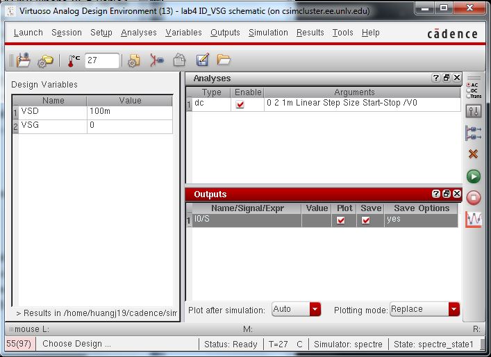
Run the dc response and you should get the following.
Now let's layout a NMOS and PMOS.
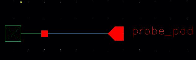
First we have to create a probe pad.
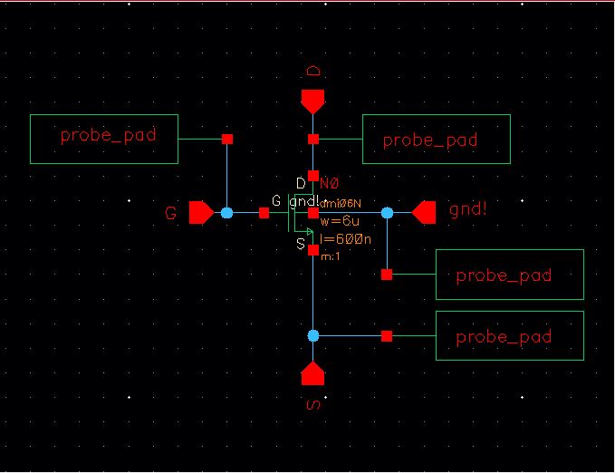
Create a new schematic cell view in your lab 4 named probe_pad.
Draw the following schematic.
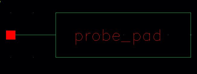
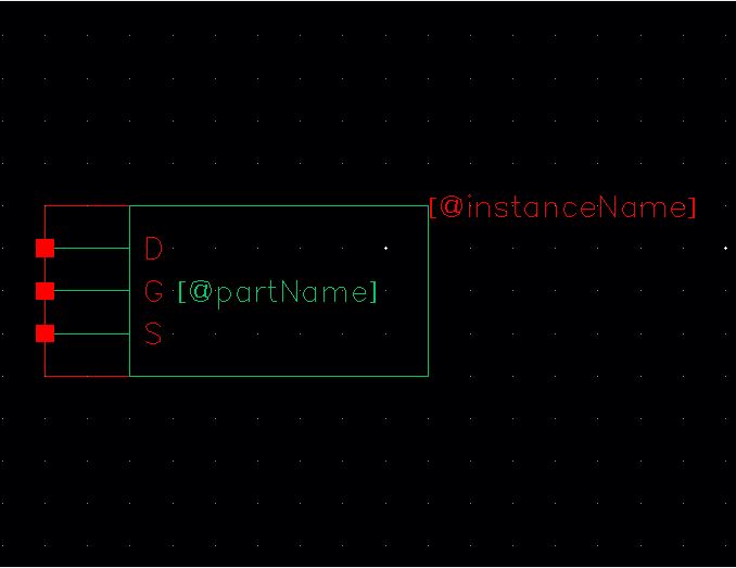
Create
a symbol from the cellview and delete everything except what you see
below. This is now our symbol for a probe pad we can use in the
schematic of our NMOS and PMOS.
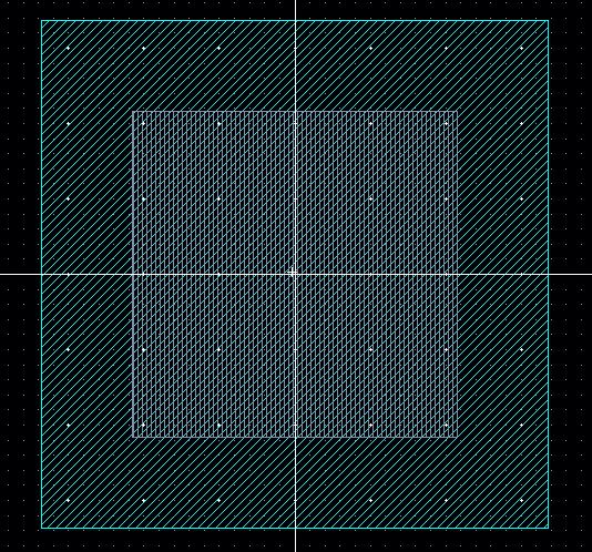
Create a new layout view in your probe_pad cell and layout.
Lay out a sheet of n-well that is made out of metal3 that has a width and height of 33.6um.
And lay out an over glass that 21.6um square.
Now let's start with a NMOS layout.
We are going to layout a 6u/0.6u NMOS and connect all of 4 MOSFET terminals to probe pads.
Create a new schematic view called 6u_600n_NMOS.
Draw the following schematic using the NMOS from Tutorial_2 and the probe_pads symbol you just created.
Check and save your schematic.
While we are at it we can create a symbol from your cellview of the schematic.
We can use this symbol we created later on if we need it.
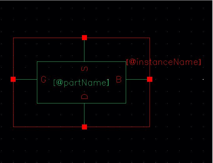
It should look like the following below.
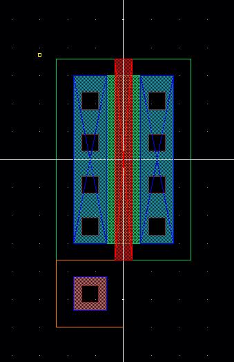
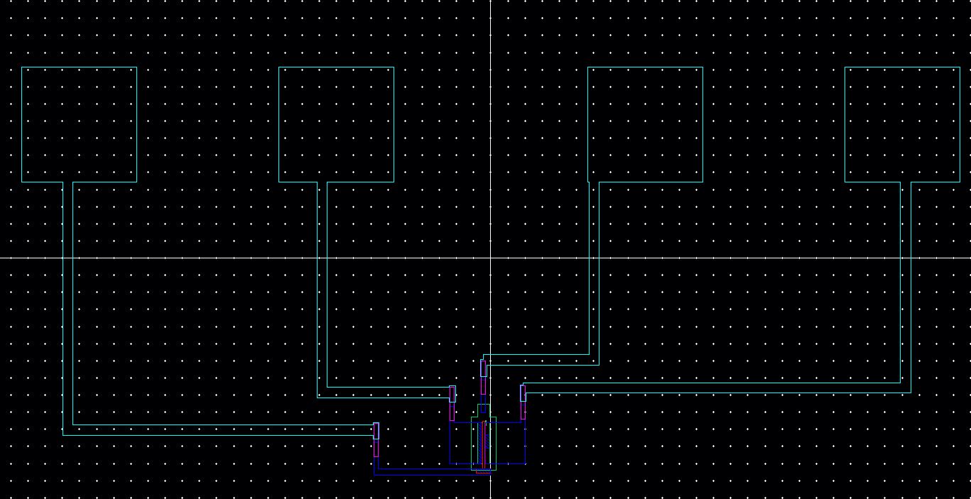
Create a new layout view and lay out the following layout.
We are using the layout probe pads we created before and the NMOS we created in Tutorial_2.
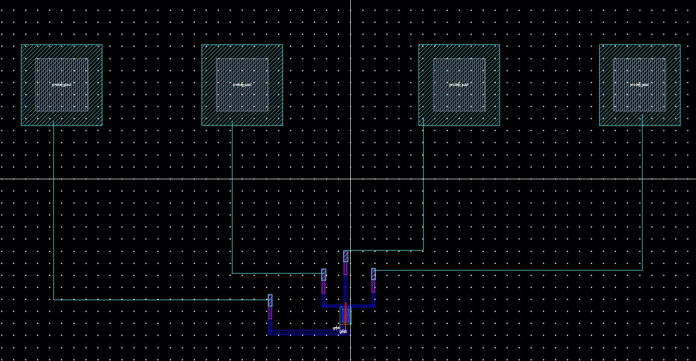
Connect the Source, Drain, Gate and gnd! with metal 1 pins to ptap contacts.
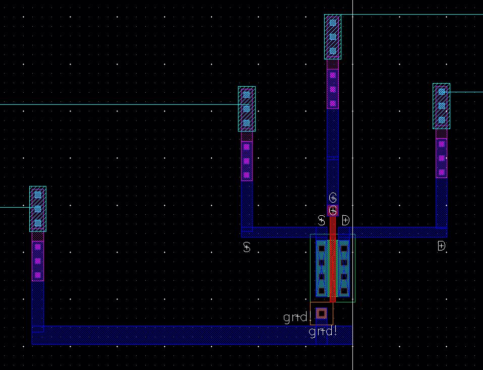
DRC your layout and make sure there are no minimum width or spacing errors.
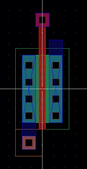
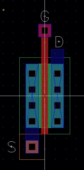
Save and extract your layout.
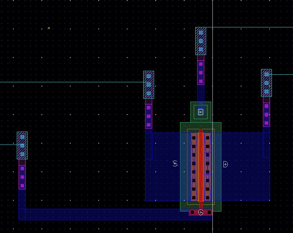
Open your extracted layout and it should look like the following.
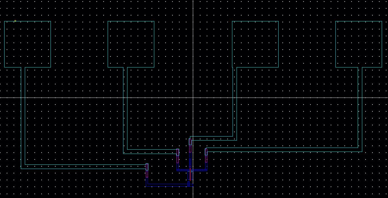
Zoomed in view of your extracted NMOS.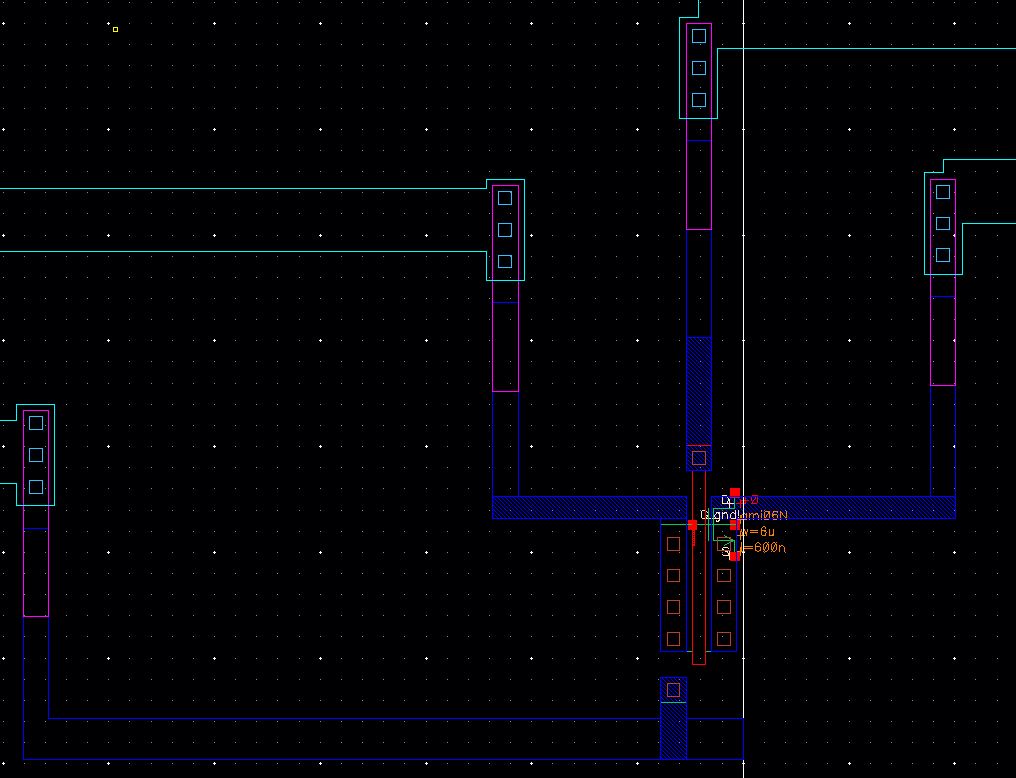
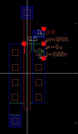
Now LVS your extracted view with the schematic view you created earlier.
Make sure you select the correct extracted and schematic file.
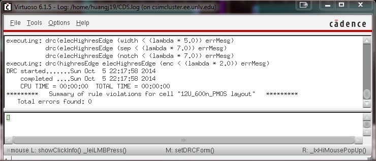
Run the LVS.
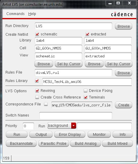
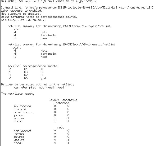
Your LVS should match your netlist should match as seen below.
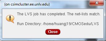
Now you can click Output in your artist LVS window and verify that the net-list match.
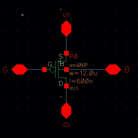
Now let's make a PMOS layout.
We are going to layout a 12u/0.6u PMOS and connect all of 4 MOSFET terminals to probe pads.
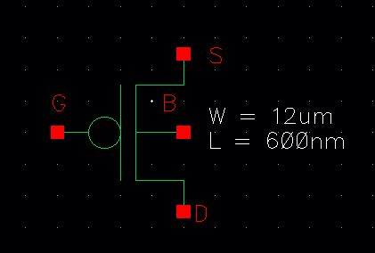
Create a new schematic view called 12u_600n_PMOS.
Draw the following schematic using the PMOS from Tutorial_2 and the probe_pads symbol you just created.
Note that the pin labeled B is your vdd! pin.
Check and save your schematic.

Again since we created the schematic we can create a symbol for your PMOS.
It should look like the following below.
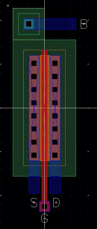
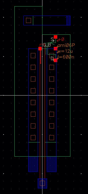
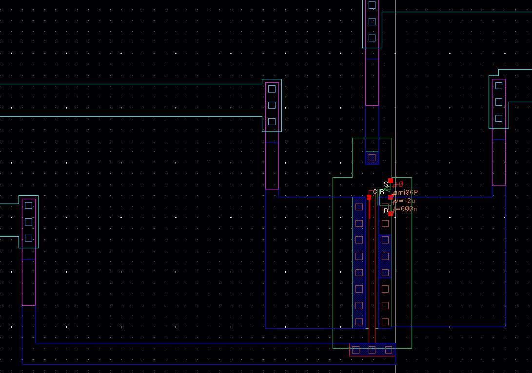
Create a new layout view and lay out the following layout.
We are using the layout probe pads we created before and the PMOS we created in Tutorial_2.
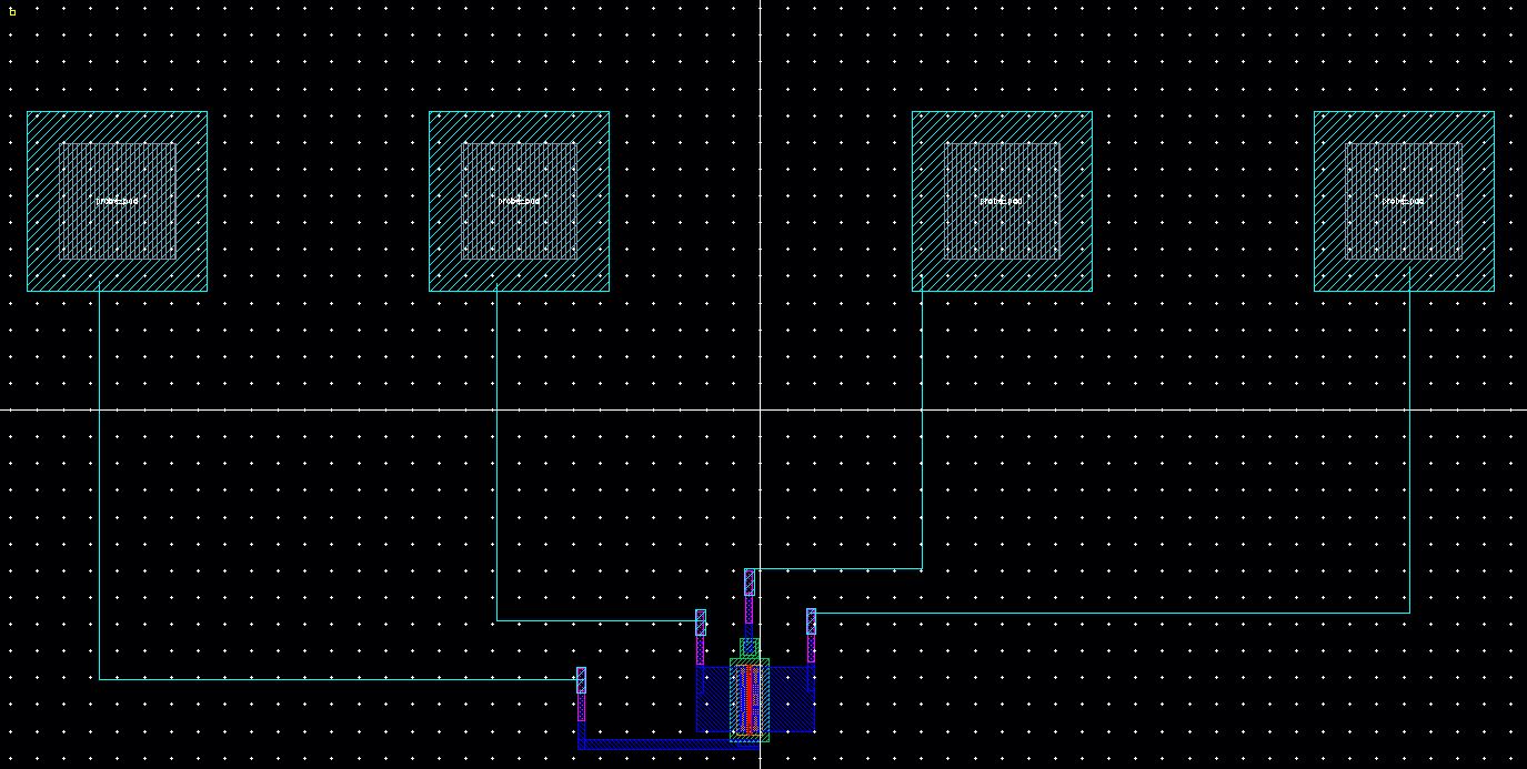
Connect your Source, Drain, Gate, and vdd! (labeled B in the layout and schematic) with metal1 pins.
DRC your layout and make sure there are no minimum width or spacing errors
Check and save your layout.
Now we can extract our layout.
Open the extracted view of our PMOS.
Zoomed in view of our extracted PMOS.
Now LVS your extracted view with the schematic view you created earlier.
Make sure you select the correct extracted and schematic file.
Run the LVS.
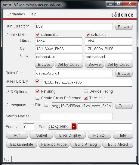
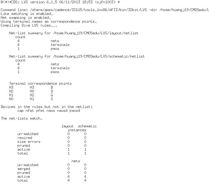
Your LVS should complete and your netlist should match as seen below.
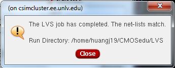
Now you can click Output in your artist LVS window and verify that the net-list match.
All of the files from this lab can be found here.
Now back up your lab by zipping it up and send it to yourself through email!
Return to EE 421L Labs