Lab 3 - ECE 421L
Now lets continue from where we left off in lab 1.
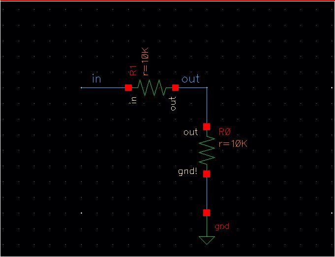
Now add another line from the output of the first resistor like below.
Check and save your schematic.
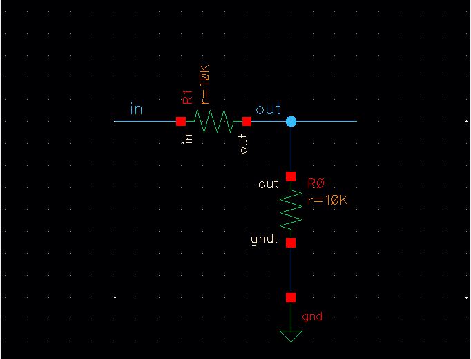
Now let's create a symbol for this schematic.
Go to Create -> Cellview -> From Cellview
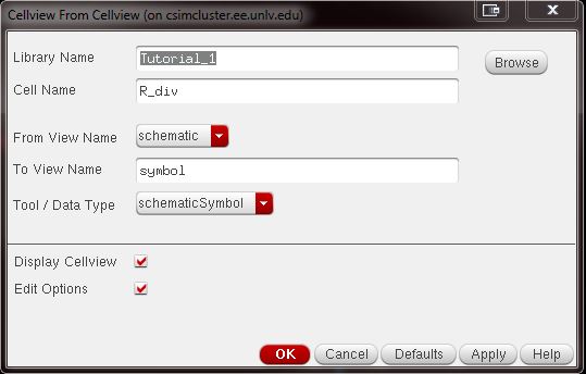
Click OK and you will be prompted with this window below.
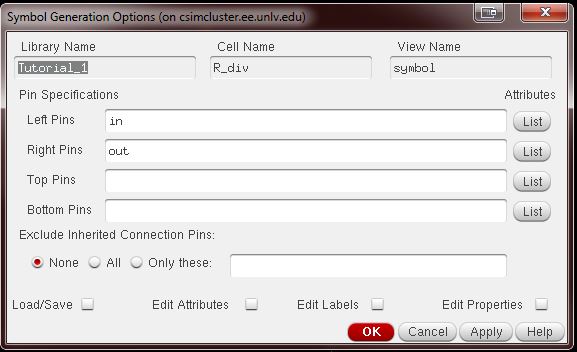
Make sure you label your pins according to your schematic in the boxes.
Click OK and you will get the following below.
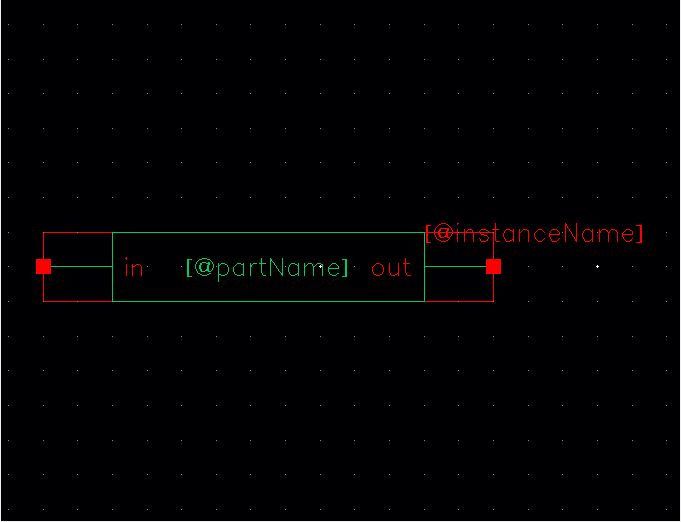
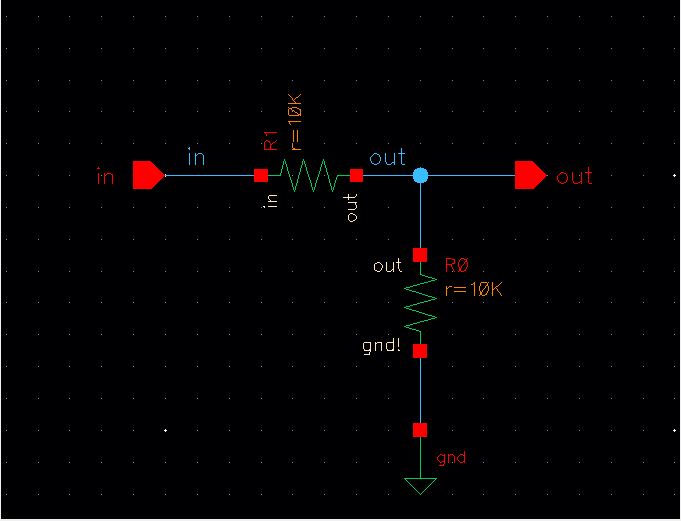
Delete everything except for the in and out pins.
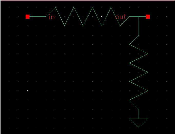
Now add a line by going to Create -> Shape -> Line and draw the symbol seen below.
Check and save the symbol and close out of the symbol and schematic views of the R_div cell.
Now go to your Library Manager and copy the R_div cell.
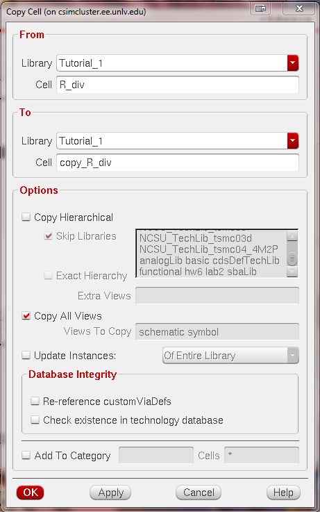
After hitting OK delete the spectre_state1 in the R_div cell and delete the symbol view in the copy_R_div cell.
Now open the schematic view of the copy_R_div cell and delete everything in the cell.
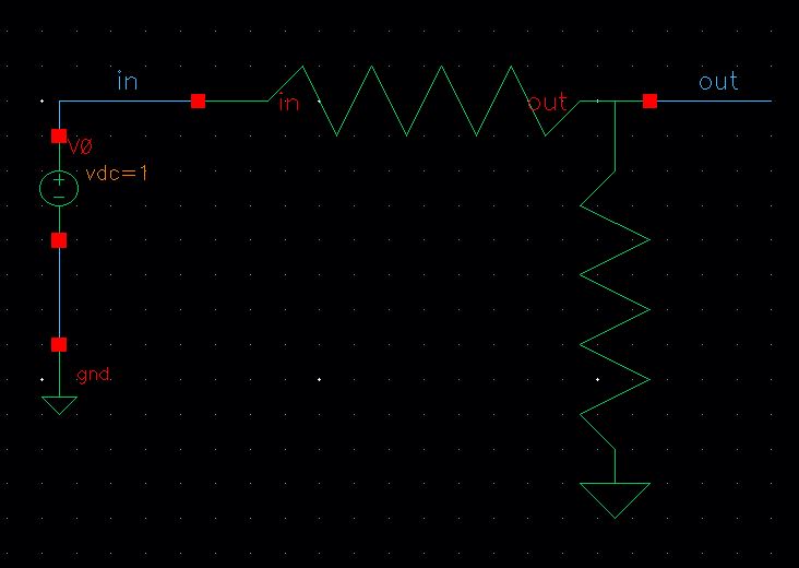
Add an instance of your symbol of R_div from your Tutorial_1 library as seen below.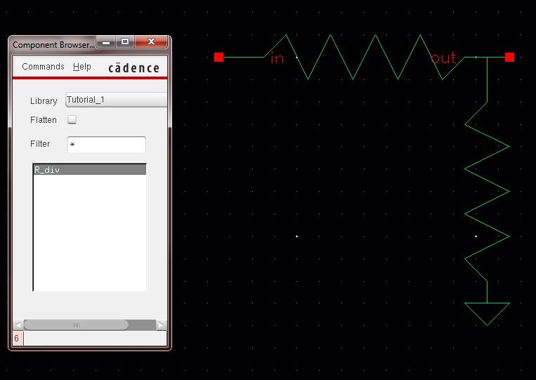
Now add wires and components as seen below, setting the input DC voltage to 1.
Check and save the schematic and you will find two warnings.
These warnings are for the floating wire name out.
Go to menu Check -> Find marker to see the details.
Since we want these wires to be floating, ignore these two warnings and click Apply.
Check and save the schematic again.
Launch ADE and load the state from cellview and run the transient response.
Let's start creating shapes in the layout.
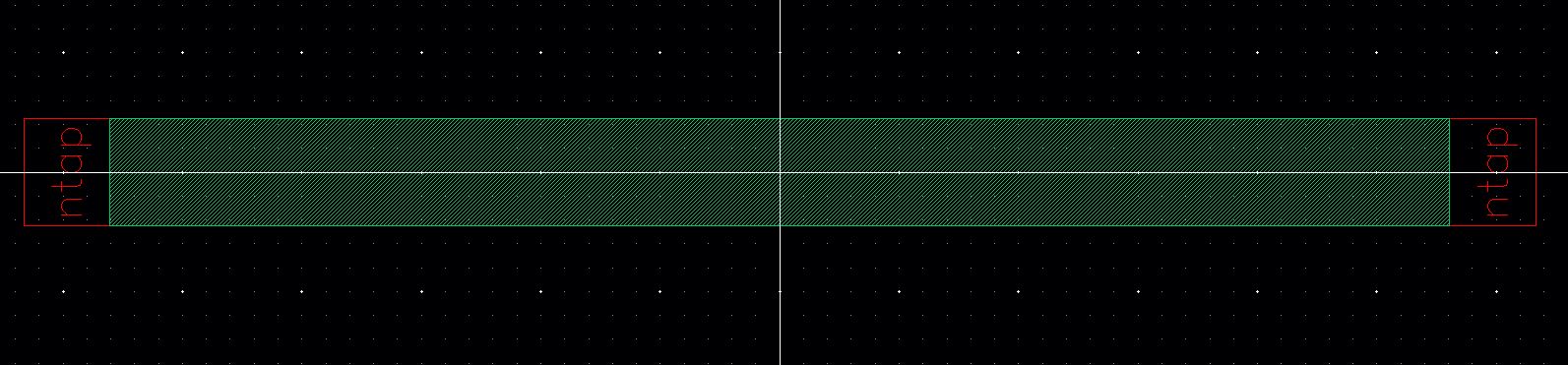
We are going to create a 10k resistor using n-well in layout.
The sheet resistance of the n-well in the C5 process is about 800 ohms.
Note that there are design rules for n-well. The minimum width is 12 lambda (3.6 microns with lambda being 300 nm).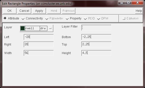
Design Rule Check (DRC) the layout by going to Verify -> DRC and hitting OK.
In the CIW we see that there are 4 errors.
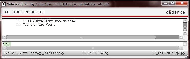
Go to Verify -> Markers -> Find Marker and check Zoom to Markers and click Apply.
We get the following zoom in of our n-well rectangle.
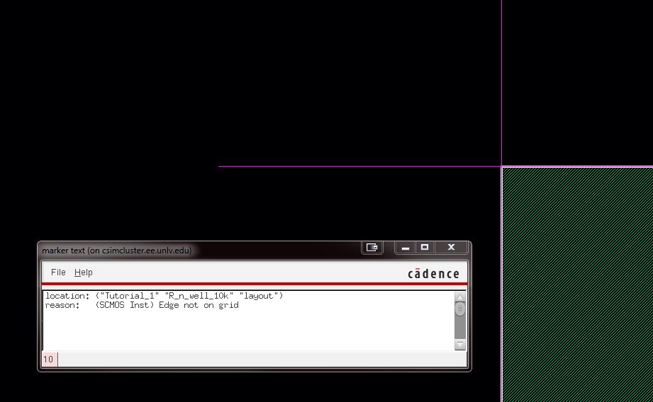
Close the marker text window and zoom out until you can see the grid.
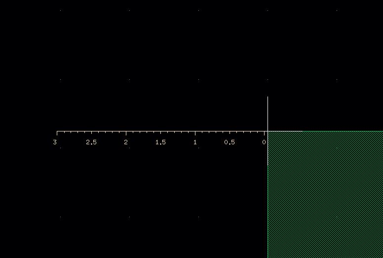
Let's create a ruler to measure the grid by going to Tools -> Create Ruler (bindkey k)
We can see that our rectangle is not snapping to 0.15 microns.
Clear the rulers by pressing K (shift + k)
Press f to fit the screen and click on the rectangle and go to its properties.
Since the length is currently 56/0.15 = 373.333 this is not a whole number which means this is not a factor of 0.15 microns.
We can increase the length to 56.1 since 56.1/0.15 = 374. Change the Left and Right values to 28.05.
For the width it is 4.5 but since 4.5/0.15 = 30 it does correctly fit the 0.15 micron requirement.
Run DRC and you will receive no errors.
Now we can add connections to the end of our n-well resistor.
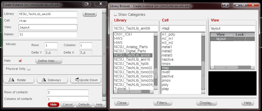
Press i to create an instance and navigate to ntap which is in the NSCU_TechLib_ami06 library.
Make sure you are changing the rows of contact to 2.
Before placing your ntaps, check if your gravity is on by pressing E (shift+e).
Gravity helps create affinity of your nodes to similiar layers.
Place your ntaps and move them to where you placed your n-well rectangle.
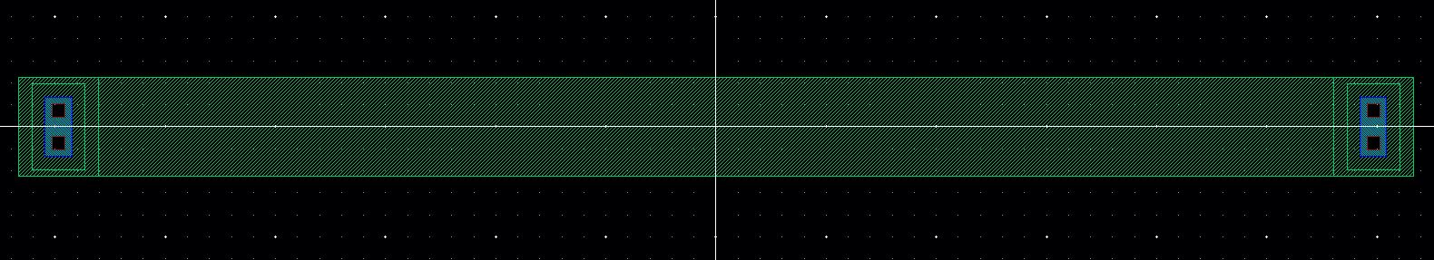
Notice your ntaps are only outlines.
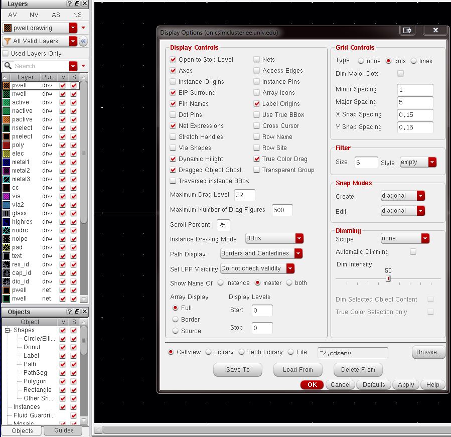
You can change this by changing your display level in your display options to 10.
DRC your layout and ensure there are no errors.
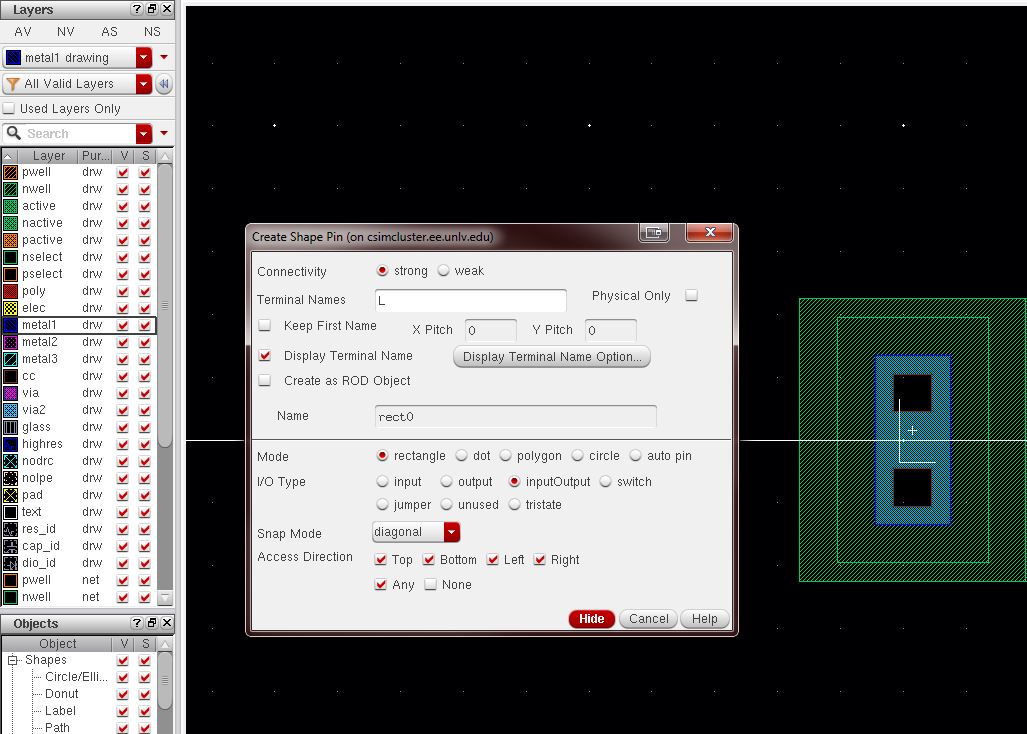
Now we can add pins to the layout.
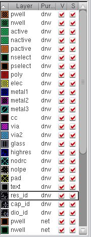
Select metal 1 in your LSW.
Go to Create -> Pin and select Display Pin Name.
Name your left pin L and your right pin R.
Draw your pins ontop of your metal 1 rectangle on your ntap.
Next select the layer res_id (identify resistors) in your LSW.
Draw a rectangle ontop of your n-well rectangle you drew before.
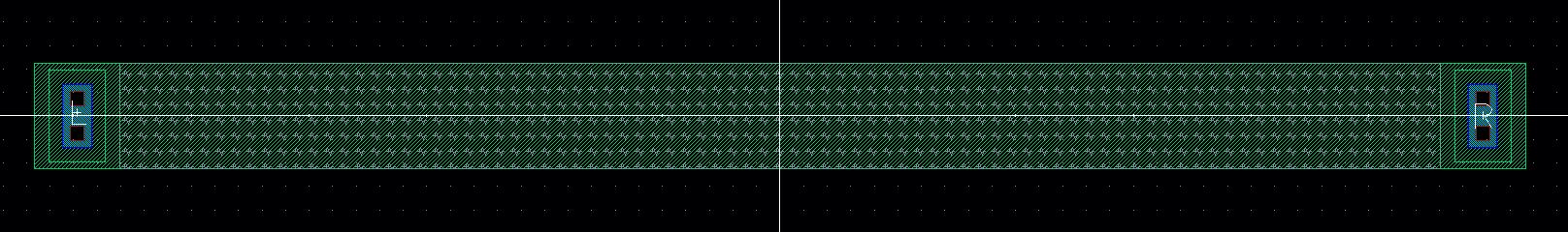
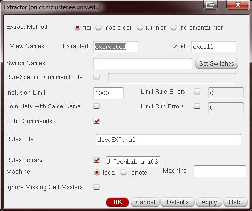
Lets extract the layout to determine the resistance value.
Go to Verify -> Extract and click OK.
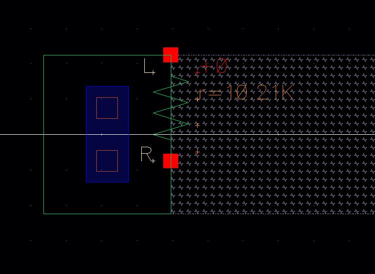
Go to your Library Manager and open the extracted view in your R_n_well_10k cell.
Zoom in and you will see your resistors value is 10.21k.
Close the extracted view.
Save and close the layout view of your resistor.
Open the layout view for the R_div cell
Instantiate two of the 10k n-well resistor layouts
DRC your layout to make sure you have adequate spacing between the resistors.
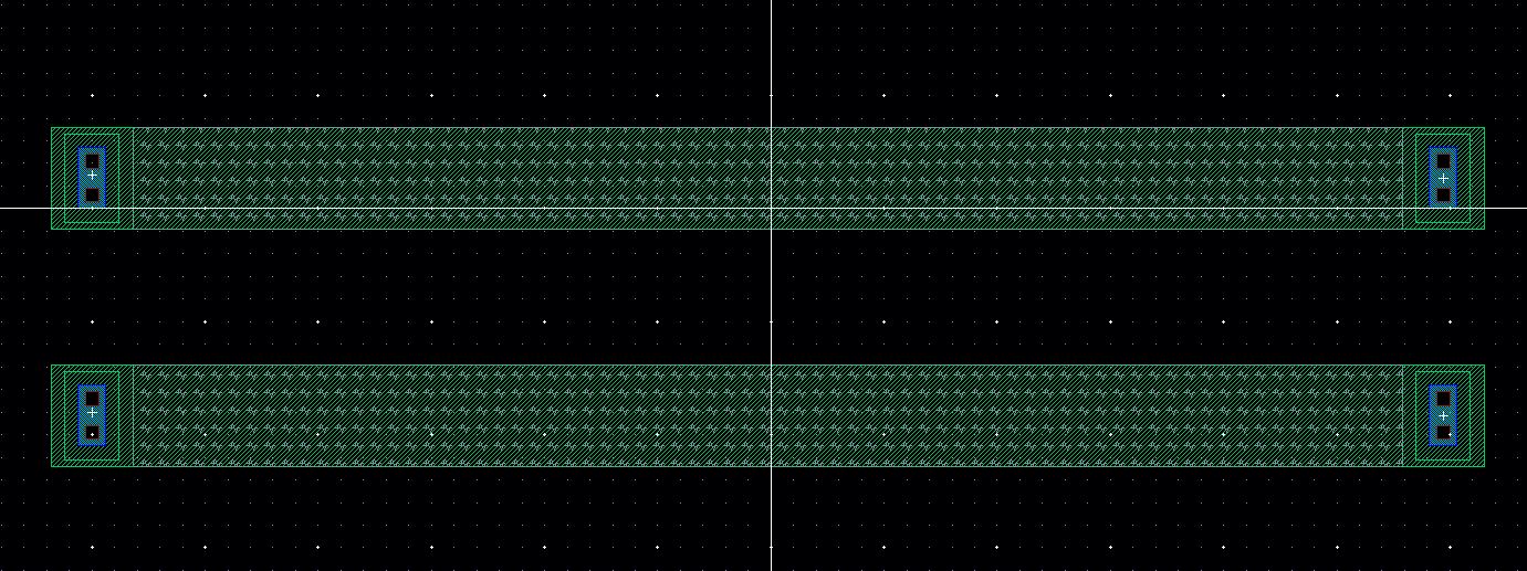
Next select metal 1 in your LSW and add rectangles to connect the resistors together by placing them on the pins as seen below.
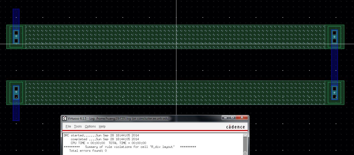
DRC the layout to ensure there are no errors.
Next add pins to your layout by using metal 1 and creating pins in, out and gnd.
Make sure your pins are the same size as the metal 1 rectangle connections you made in the previous step.
DRC your layout.
Extract your layout.
Now go to Verify -> LVS
Select your extracted R_div and your schematic R_div in the property spots as seen below.
Hit Run
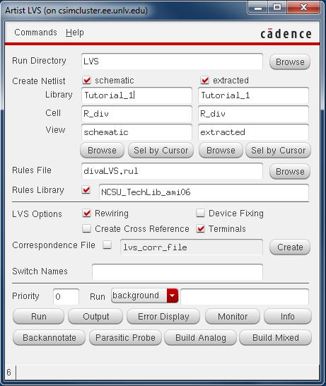
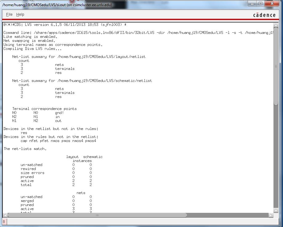
You will get notified that the LVS suceeded to run but the schematic did not match.
Press Output in your LVS window and scroll down and you will see the following below.
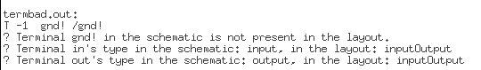
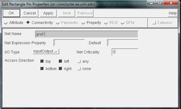
This occured because we did not label our ground pin correctly, we need to name it gnd! (the excalmantion point indicates a global value)
We also have to change our I/O type to input in our in pin and output in our out pin
Change these errors and DRC, Extract and LVS one more time you should you have a succeeded LVS and a matching schematic!
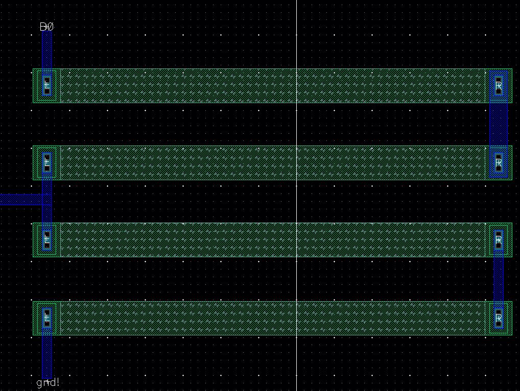
Using the n-well layout resistor from R_n_well_10k cellview we can create the 10-bit DAC we used in lab 2.
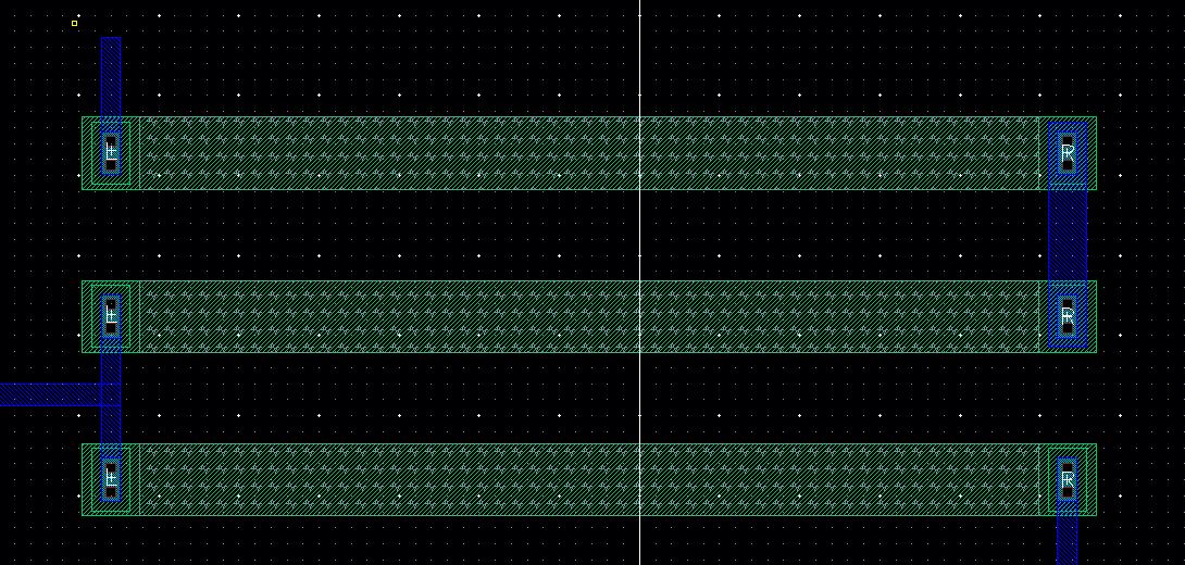
First we create a new cellview layout called lab3 and instantiate three 10k n-well resistors.
We can use metal 1 to connect the three 10k resistors as shown below.
This gives us a two 10k resistors in series and one 10k resistors in parallel. This is the 2R/R we need for our DAC.
Notice we have a left rectangle on the right where it will be an output where it will make the resistors parallel.
We can repeat this process 10 times to create our 10 bits for our DAC.
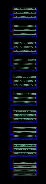
Now we can create our pins for our schematic.
Shown below is where B0 (input pin) is and where our 2R/2R from our DAC where it ends with a ground (gnd!) pin.
Note that the B9 pin on the top of our design will have a Vout pin to the left of the schematic.
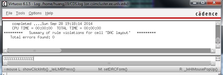
We can now DRC this schematic and get 0 errors.
Extract the layout and now we can LVS the design.
Selecting the extracted cellview from the previous step and the schematic view of our ideal 10-bit DAC we created in lab 1 we can LVS our layout.
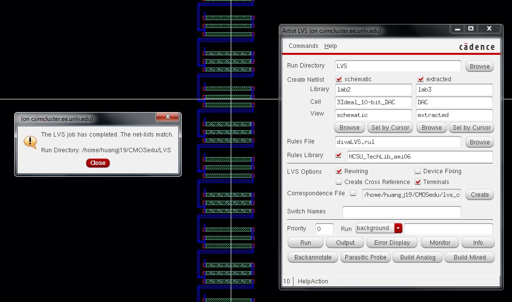
We can see that the net-list match for our layout design of the 10-bit DAC.
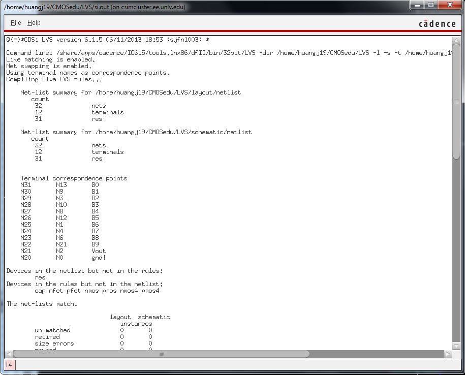
We can open the Output of the LVS and see that the netlist matches.
We can determine the width and length of the resistor by using the equation of a resistor using R = L/W x Rsq where Rsq is the sheet resistance of the material, in this case it is 800 ohms in the C5 process.
If we rearrange the equation looking for L/W = R/Rsq
Where R = 10k ohms and Rsq = 800 ohms
We get the ratio of L/W to be 12.5
Letting us really pick any value of length and width be whatever aslong as the ratio is around 12.5
For our 10k n-well resistor we used 56.1 microns for the length and 4.5 microns for the width which is 56.1/4.5 = 12.4666
Since we used the 10k n-well resistor we created for the 10-bit DAC we already know the measurements of each 10k resistor.