Lab 2 - ECE 421L
Authored
by John Huang.
Huangj19@unlv.nevada.edu
September 15, 2014
In this lab we will use n-well resistors to implement a 10-bit DAC.
First back up all of your previous work.
Now let's download lab2.zip to your desktop.
Upload this zipfile into your design directory in your server that you're running Cadence from.
Unzip this directory and add this statement into your cds.lib file
- DEFINE lab2 $HOME/CMOSedu/lab2
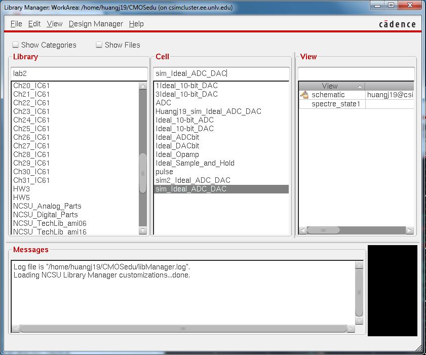
Start Cadence and use the library manager to navigate to lab2 library and open this sim_Ideal_ADC_DAC
Launch ADE and load the state and run the transient response.
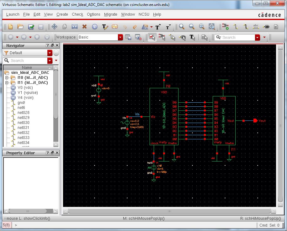
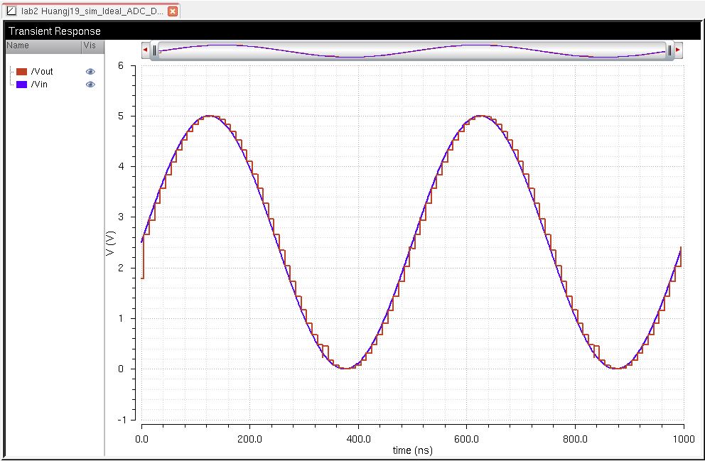
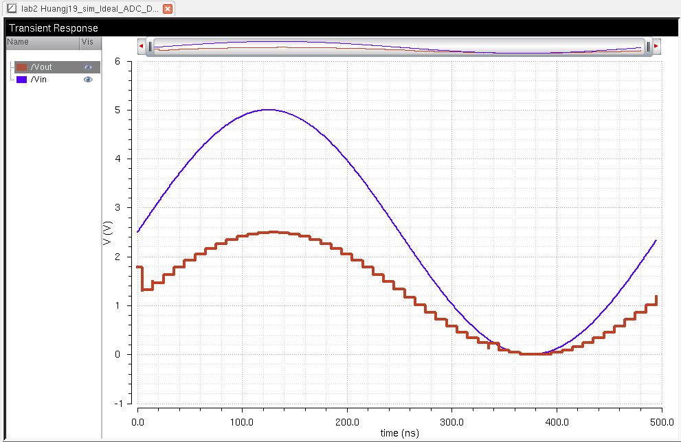
Your simulation should look like the following.
The general concept of the ADC and the DAC is to convert a digital signal into a discrete signal.
Note that the least significant bit (LSB) is the smallest voltage capable of being quantified in our circuit.
We
can find the LSB by finding the smallest bit value we can use in our
circuit, this would be 1/(2^N) where our N is 10 because it is a 10 bit
ADC to DAC.
This
results in 1/1024. Now we can tak this smallest bit value and multiple
by our highest voltage we can supply for our circuit, 5V. This gives us
5/1024 volts which approximates to 5mV.
Now knowing all this information, we can continue on building our circuit.
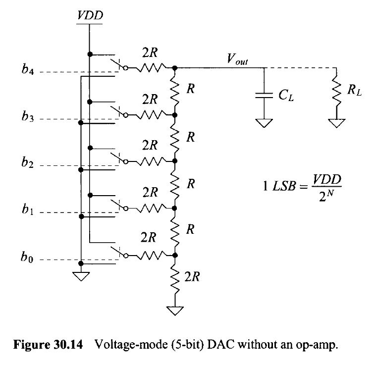
Our design will be implemented using Fig 30.14 from the CMOS book.
In order to create this 10-bit DAC we first must create a symbol using n-well.
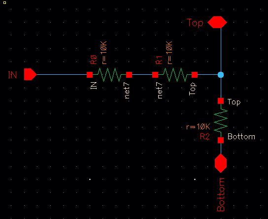
In Virtuoso, make a new schematic cell view and name it R_div.
We will place two 10k resistors in series and one 10k resistor in parallel to create a resistor divider.
Place input/output pins (bindkey p) in the corresponding places shown below.
Check and save the schematic, make sure there are no errors before proceeding to the next step.
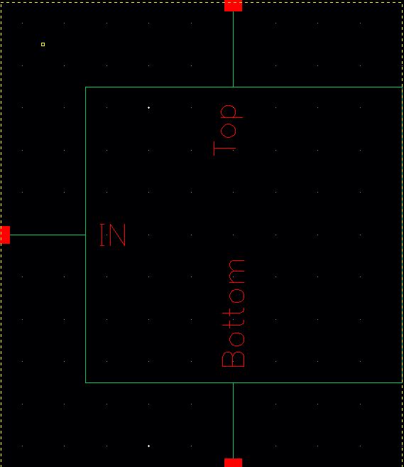
Now to create the schematic into a symbol go to Create -> Cellview -> From Cellview.
Click
okay to finalize the cellview schematic symbol, and in the Symbol
Generation Options label correctly the Left, Right, Top, and Bottom
Pins. In this case you will not have a Right Pin.
Click okay and you should have a symbol similiar to the picture below.
Now copy the 10-bit Ideal DAC symbol from inside the folder
Descend into the edit hierarchy (bindkey X) of the symbol. Note: if you use bindkey x you will descend into the hierarchy but in read only mode.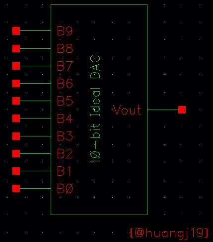
Delete everything inside the 10-bit DAC.
Go create an instance (bindkey i) and select in the Library where you saved your R_div from the Component Browser.
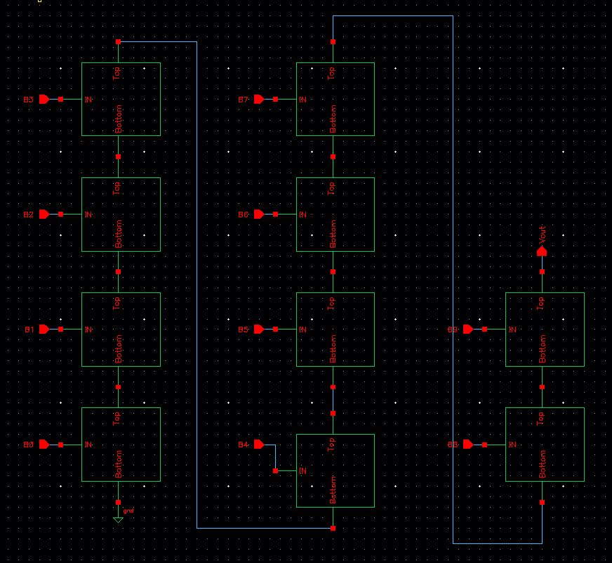
Place your R_div similiarly to the picture below.
Next connect Pins labeled B0:B9 from the IN Pin from the R_div symbol.
Also connect the Top and Bottom Pins as seen in the picture below.
Make sure you connect the B0's Bottom Pin to ground and B9's Top Pin to a Vout Pin.
Check and save the schematic.
Now return to the top layer (bindkey b).
Note: the total resistance of this circuit can be found by simply simplifiing all the resistors in the circuit.
If
we refer back to Fig 30.14 we can start from the bottom 2R resistor and
see that this resistor is in parallel with the 2R resistor.
Combining this will result in a resistance of R. This resistance R is in series with another resistor with the value R.
Combining
these resistors in series will result in 2R. Note that this will
continue until you reach the top of the figure and that your resulting
simplied resistance has a total value of R.
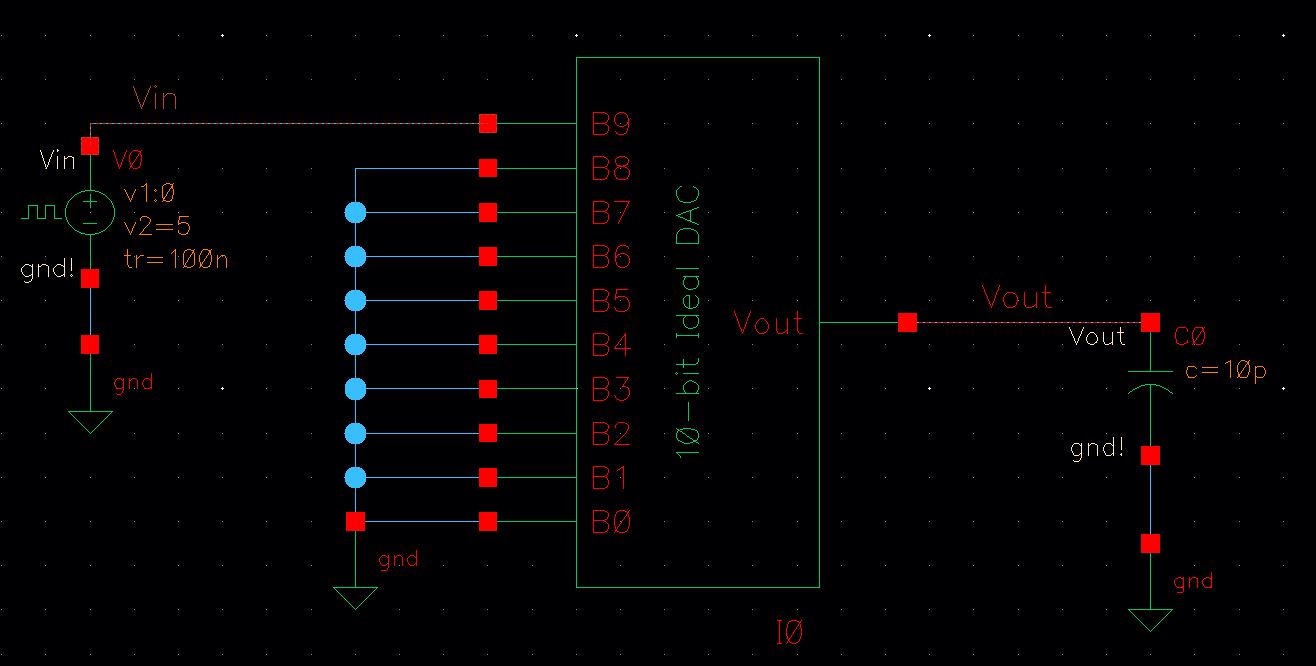
Now create a new cellview in the Library Manager and label it 10-bit Ideal DAC Pulse.
Create an instance and add the 10-bit Ideal DAC you just created.
Ground all the DAC inputs except B9.
Connect B9 to a pulse source (0 to 5V).
Add a load to Vout by placing a 10pF capacitor parallel to Vout.
Check and save.
Launch ADE and go to Analyses and run a transient response for 4us.
Make sure you select your Vin and Vout for outputs to plot.
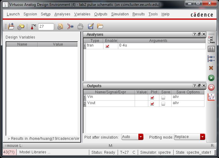
Run the transient response and you should get the following graph.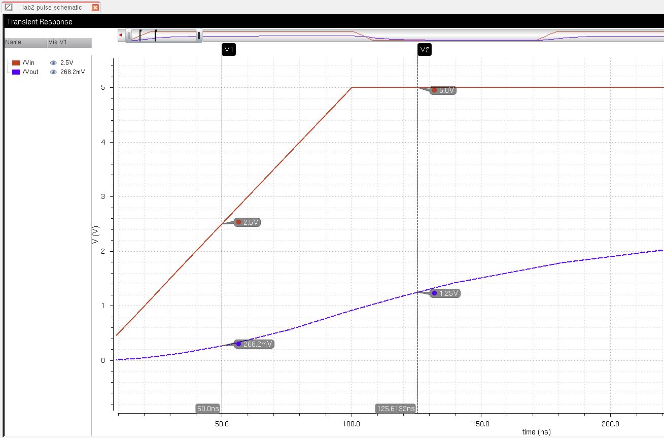
The following graph shows the delay from adding a load to the DAC.
From measuring the time it takes to reach 0.5Vin and 0.5Vout we can find the time delay.
It is measured that Vout is at 125.6ns at 1.25V and Vin is at 50ns at 2.5V.
125.6ns - 50ns = 75.6ns = td = time delay.
We can also compare this to our hand calculations of time delay.
We can calculate this time delay by using the formula that td = 0.7RC.
We know that the resistance value of the 10-bit DAC is 10k from the earlier and that the capacitance is 10pF.
td = 0.7RC
td = 0.7(10e3)(10e-12)
td = 70e-9 = 70ns
Our simulation results and our theoretical results are very accurate.
Now we can verify our design functions correctly.
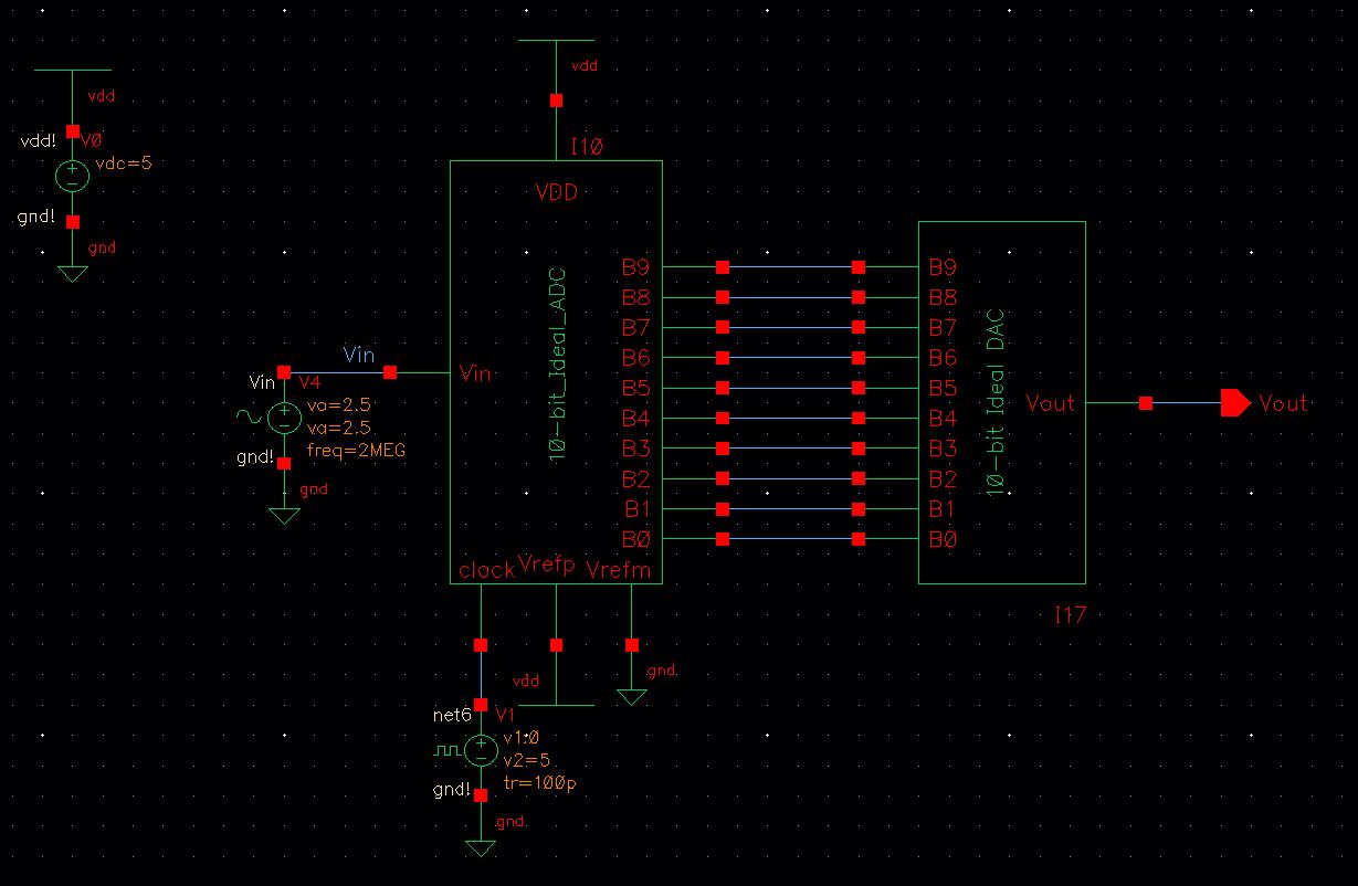
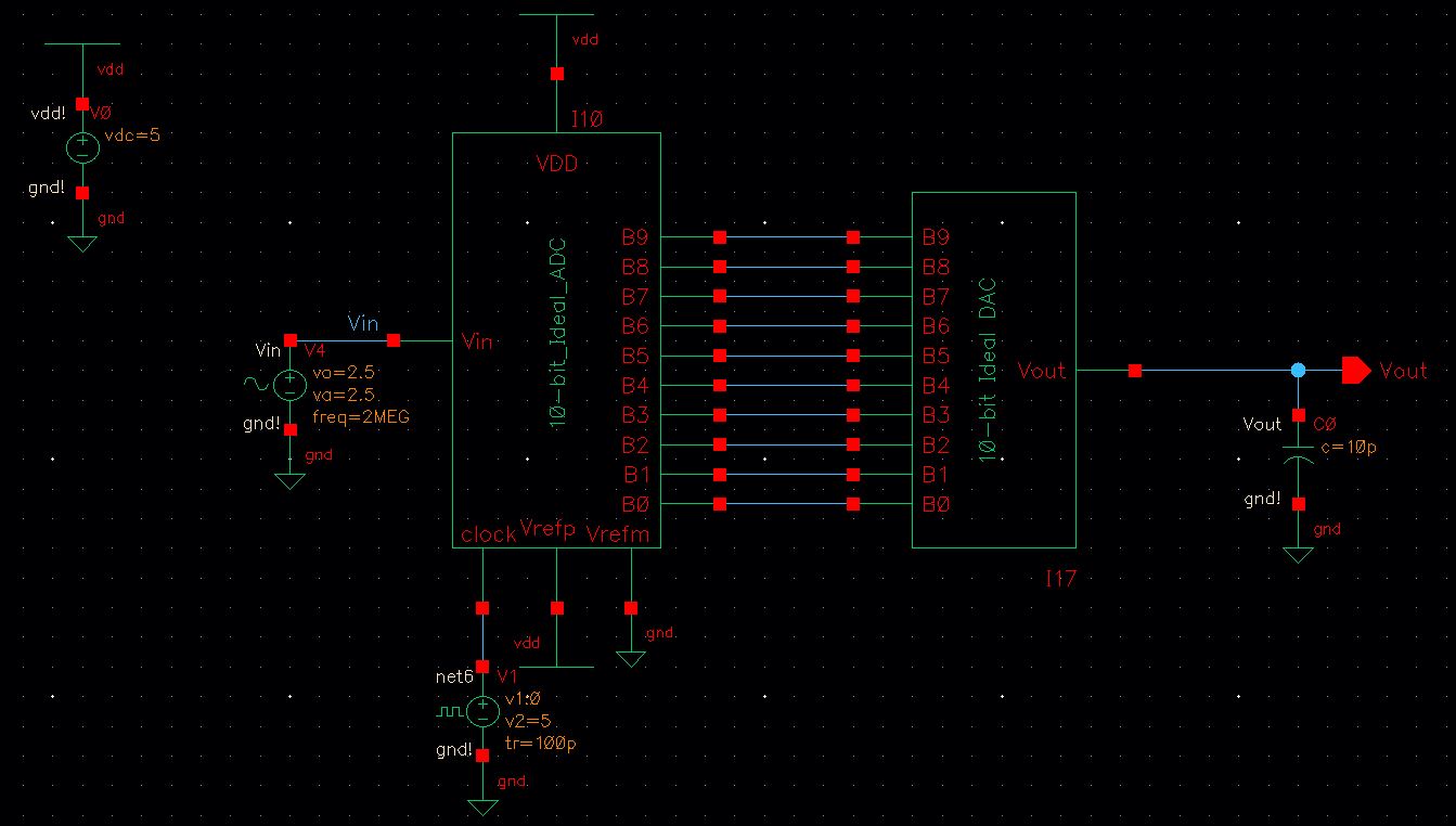
Start by copying
the schematic cell view sim_Ideal_ADC_DAC to a cell sim2_Ideal_ADC_DAC
and replace the ideal DAC with the one you created previously.
Look
at the picture below. Make sure you do not have the VDD, Verfp, or
Vrefm in your schematic for your DAC as we will not be using those with
our symbol.
Check and save.
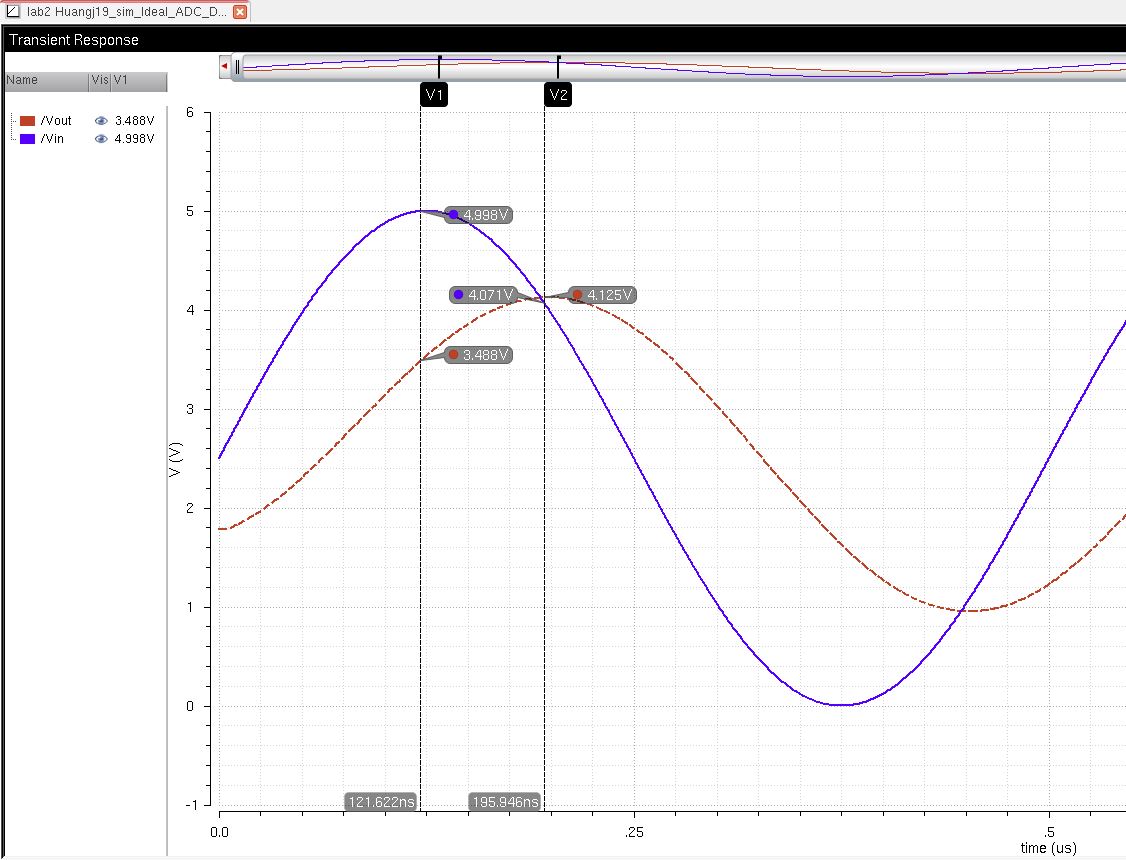
Launch ADE and load the cell view state and run the transient response.
Your
response should look like the following picture which is the same as
the one at the beginning of this lab, which verifies that your
schematic is working correctly.
Now we can create drive different loads to the ADC to DAC and observe what happens.
First we can drive a 10k resistor load. Add a resistor in parallel to Vout.
Check and save.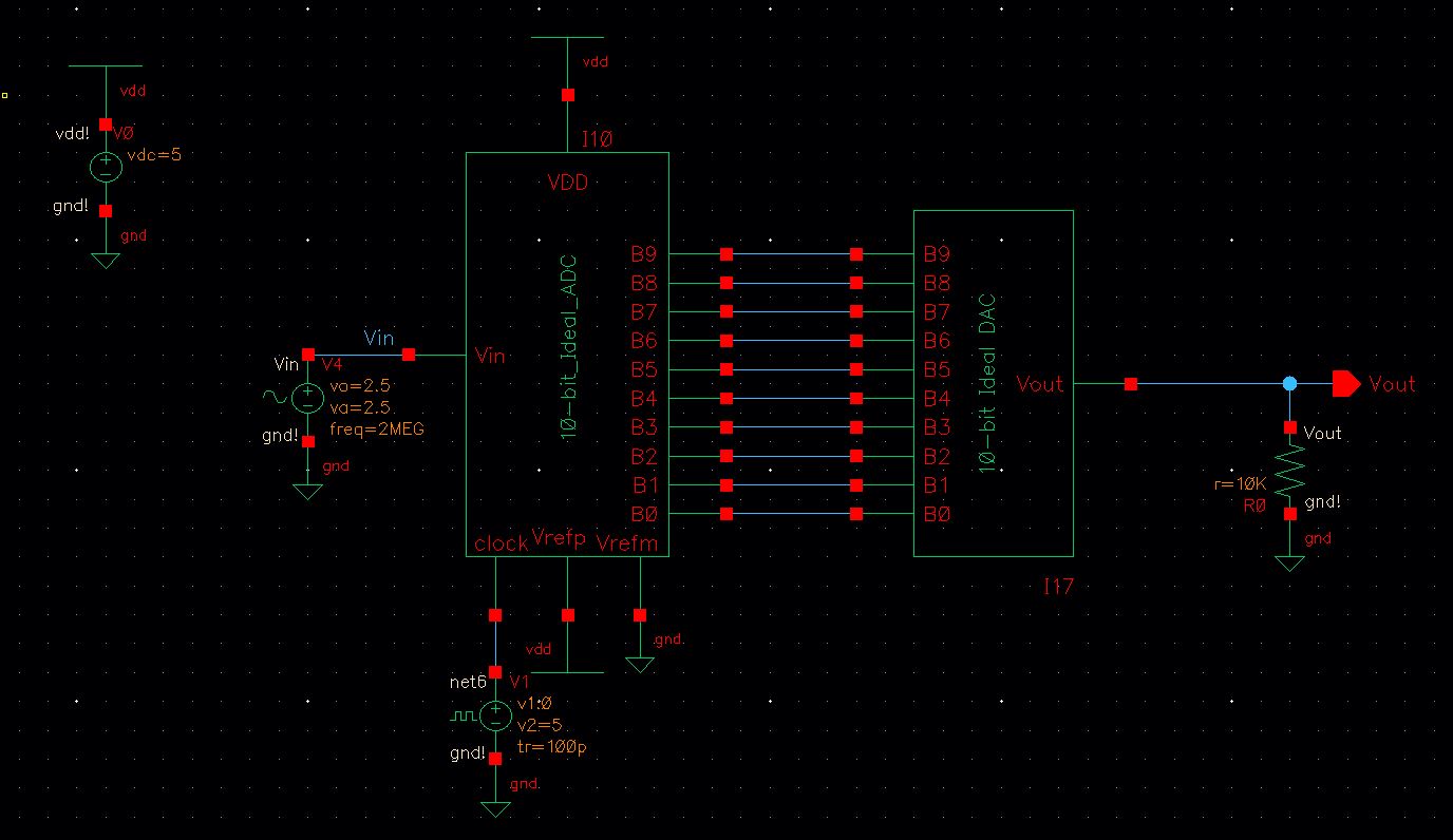
Launch ADE again and load the state and run the transient response.
We can see that adding a resistor will half Vout because it will act as a voltage divider.
Remember
we the total DAC's resistance was 10k, by adding a 10k resistor in
parallel we are basically creating a voltage divider which will half
whatever goes in, in this case it would be the 5V from Vin and thus
Vout is 2.5V
Now we can attempt to load a 10pF capacitor.
Add the capacitor, check and save the schematic.
In ADE run the transient response again and you will get the following graph.
We
can see that the capacitor will actually delay and reduce Vout. This is similiar
to what happened when we added the 10pF load to only the DAC previously.
The delay can be calculated the same way that we calculated the DAC previously.
The reduction of voltage is due to the impedance that the capacitor provides in the load.
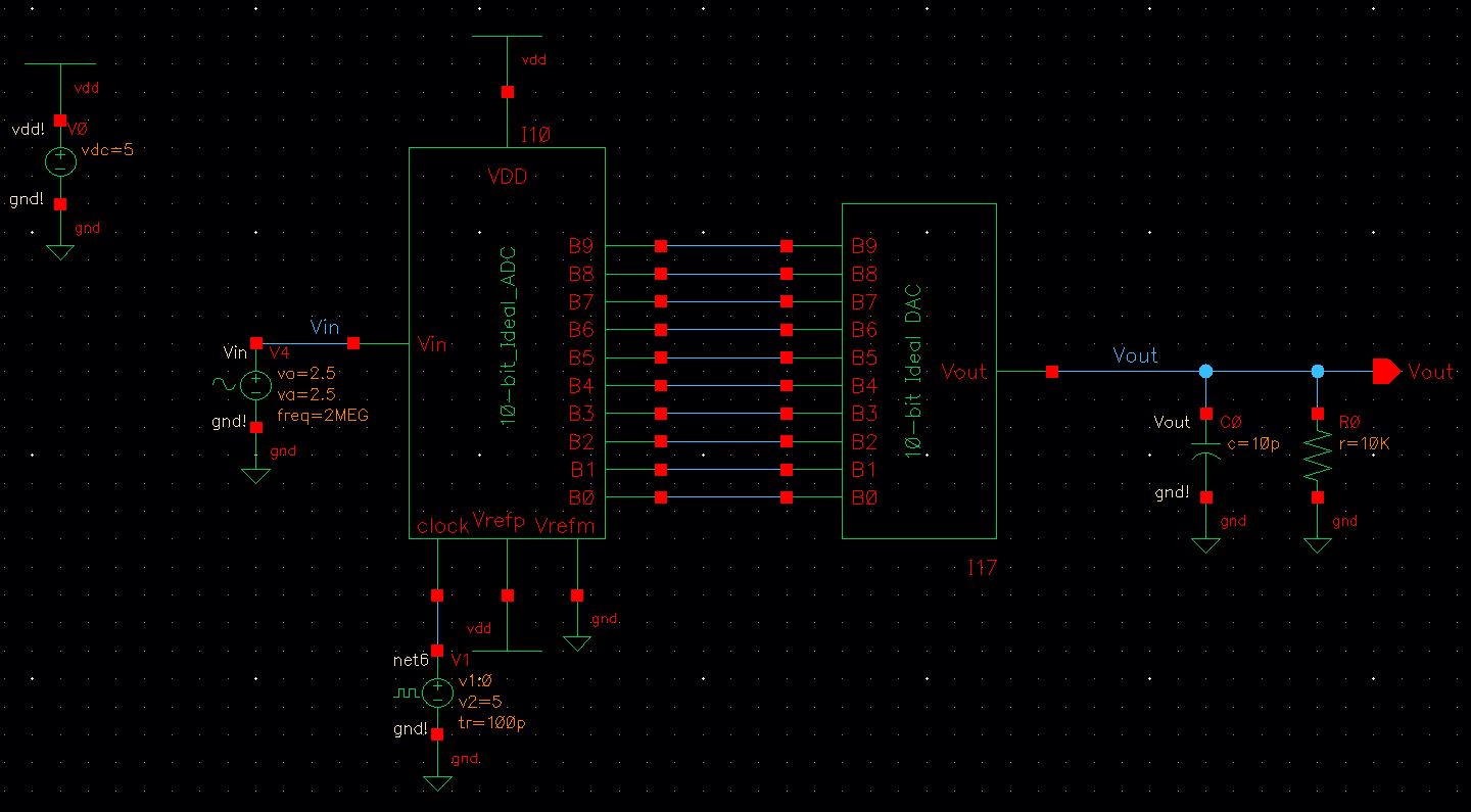
Finally we can load an R/C.
Add a 10pF capacitor and a 10k resistor in parallel.
Check and save.
In ADE we have to change the transient response time to something larger to see the response.
In this case I ran it for 10us.
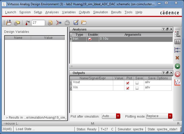
If you're having problems seeing the transient response you can try adjusting these settings in the ADE window.
Go into Simulation and select options and change the following values.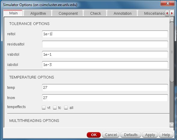
Now try running the transient response again and you should get something similiar to below.
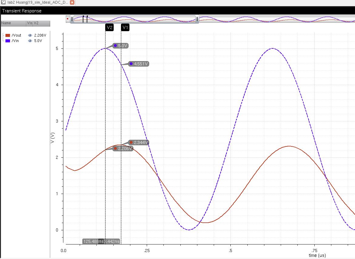
Here we can see both implementations of the resistor and the capacitor come in to play.
The output is now delayed and slightly reduced from the capacitor and output voltage is also reduced from the resistor.
In a real circuit, the switches are implemented with transistors (MOSFETs).
If
the resistance of these switches were not small compared to the
resistance of our DAC, then the switches would take voltage away from
the DAC.
This
will result in reducing the voltage output. This reduction can be found
by calcuating the output voltage by 1 - (switch resistance / DAC
resistance).
Now your lab is done.
Make sure to back up your lab again!
Return to EE 421L Labs