

Lab 7 - ECE 421L
Using buses and arrays in the design of word inverters, muxes, and high-speed adders.
LAB WORK
In this lab we will create 8-bit inverters, 8-bit NAND, 8-bit NOR, 8-bit AND, 8-bit OR gates, 8-bit 2-to-1 DEMUX/MUX, and a 8-bit full adder. First we will create the schematics, then the symbols and finally we will simulate the gates for effective operation. The 8-bit full adder will be the only design that will have a layout.
First, we create the schematic and symbol of an inverter. We will use the inverter created in lab 6. Then we eill simulate it to see the effect of a capacitive load.
Schematic | |
Symbol | Simulation Schematic |
Simulation Results | |
From the simulation it is seen that our inverter works. Also, it is observed that when increasing the capacitive load our inverter stops working properly. This happens because the inverter is not able to dissipate the charge inside the capacitor, this is an effect observed in the increase of the rise and fall time for the other capacitors.
Now we will create the schematics and symbols for the NAND, AND, NOR, and OR gates.
The NAND gate used is the gate created in lab 6. The AND and OR gates output is the output of an inverter connected to the output of an AND and OR gate respectively.
NAND (8-bit) schematic | NAND (8-bit) symbol |
AND (1-bit) schematic | AND (1-bit) symbol |
AND (8-bit) schematic | AND (8-bit) symbol |
NOR (1-bit) schematic | NOR (1-bit) symbol |
NOR (8-bit) schematic | NOR (8-bit) symbol |
OR (1-bit) schematic | OR (1-bit) symbol |
OR (8-bit) schematic | OR (8-bit) symbol |
Gates simulation | |
 | |
From the simulation results we see that our gates work properly.
Now we proceed to create a 2-to-1 DEMUX/MUX using the same schematic. In
our case, a MUX is a device that will take two inputs and will output
only one of those inputs depending on the selector. The DEMUX
takes one input and will have two outputs that will vary depending on
the selector input.
Creating the DEMUX will only require to switch A and B from input to output and Z from output to input.
MUX (1-bit) schematic | MUX (1-bit) symbol |
MUX (8-bit) schematic | MUX (8-bit) symbol |
DEMUX (1-bit) schematic | DEMUX (1-bit) symbol |
DEMUX (8-bit) schematic | DEMUX (8-bit) symbol |
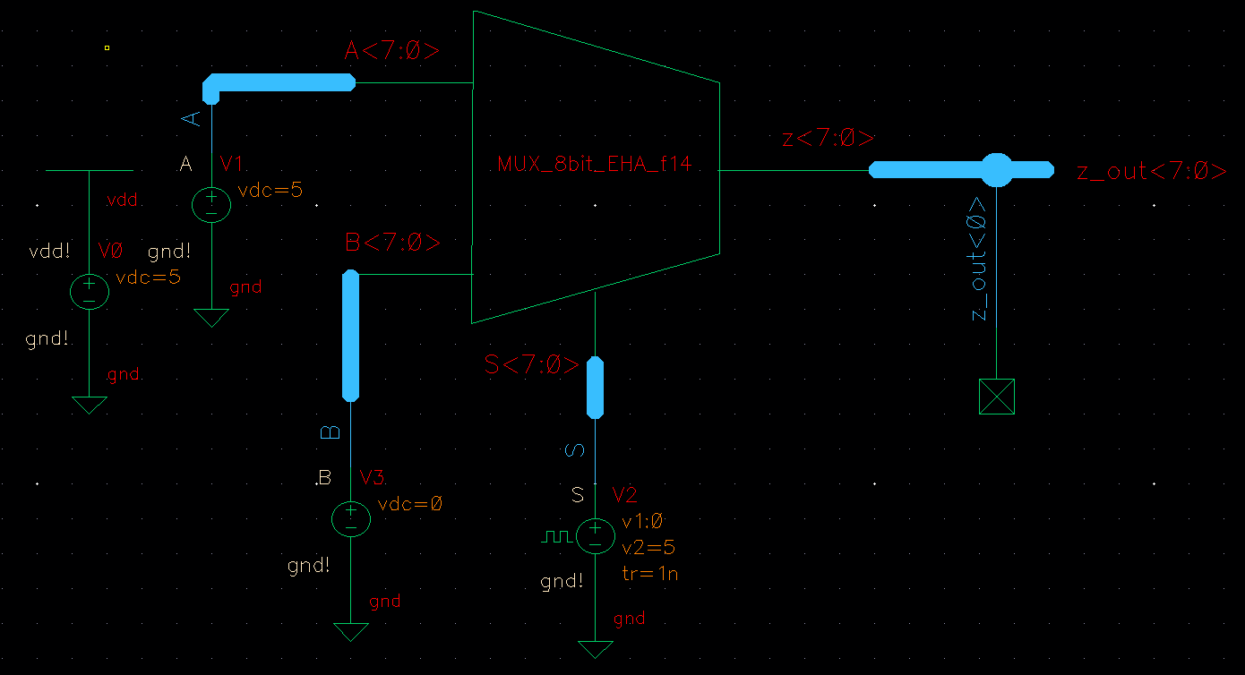
MUX simulation | MUX results |
DEMUX simulation | DEMUX results |
In our simulations it is noticed that the output of the MUX is A when S is high and B when is is low.
For the DEMUX it is seen that when S is high A=Z and when S is low B=Z.
Now we proceed to create our full adder as seen in FIG 12.20 of the CMOS book.
Full adder (1-bit) schematic | ||
Full adder (1-bit) symbol | Full adder (8-bit) schematic | Full adder (8-bit symbol |
| Full adder (1-bit) layout | ||
| Full adder (8-bit) layout | ||
| Full adder DRC | ||
| Full adder LVS | ||
Full adder (8-bit) simulation | ||
Simulation Results | ||
This lab is done and now we back up our files in Google Drive and on our desktop.
 |
Download LAB_7_ HOYUELA_EDUARDO