NMOS | PMOS |
Lab 4 - ECE 421L
IV characteristics
and layout of NMOS and PMOS devices
LAB WORK
By following tutorial 2 we will create I-V curves for NMOS
and PMOS devices.
We will start by creating the schematics we will use for the
NMOS and PMOS devices. The width is 6u and length 600n.NMOS PMOS
Then we proceed to create the layout for the NMOS and PMOS
devices. We also DRC to check there are no errors.
NMOS | PMOS |
NMOS |  |
PMOS |  |
Then we create the probe pads (metal 3 (75ux75u) with overglass (63ux63u))
Schematic | Layout |
Now we create the layout connecting the probe pads to the NMOS and PMOS
NMOS Schematic | NMOS Layout | NMOS Layout 2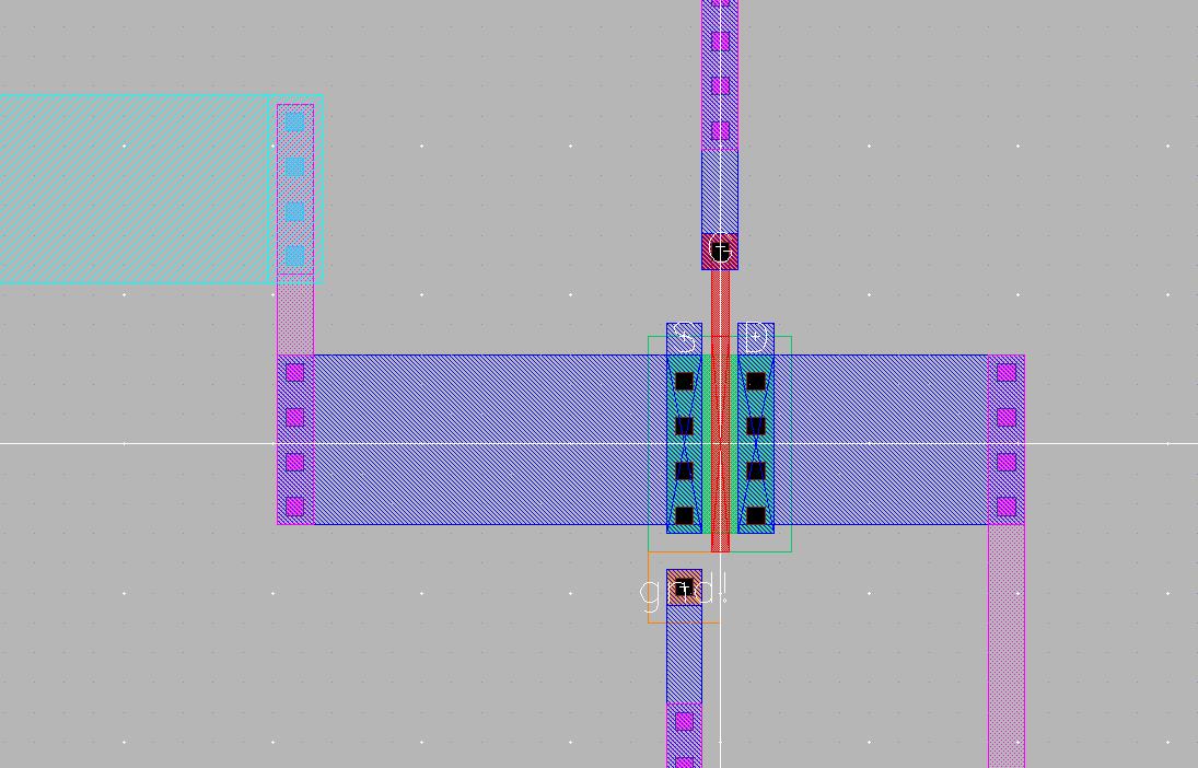 |
PMOS Schematic | PMOS Layout | PMOS Layout 2 |
We proceed to DRC and LVS
NMOS DRC | NMOS LVS |
PMOS DRC | PMOS LVS |
Now we will simulate the 3-terminal and 4-terminal NMOS and PMOS
NMOS-3 Schematic | NMOS_3 Simulation  |
|
NMOS_4 Schematic | NMOS_4 Simulation |
NMOS 4 result (VDS=100mV, VGS=0 to 2V)
|
PMOS_3 Schematic | PMOS_3 Simulation |
PMOS 3 results (VSG 0 to 5V, VDS 0 to 5V)
|
PMOS_4 Schematic | PMOS_4 Simulation |
PMOS 4 results (VDS=100mV, VSG=0 to 2V)
|
The lab is done and now we backup our files.

Download LAB_4_ HOYUELA_EDUARDO


