Lab 8 - EE 421L
Authored
by Matthew Parker (parke179@unlv.nevada.edu), Ting Yu (yut2@unlv.nevada.edu), and Leanna Guevara (guevaral@unlv.nevada.edu)
December 1, 2014
Goal
Generating a test chip layout for submission to MOSIS for fabrication
Devices included in test chip:
- 30u/0.6u NMOS (3 pins, DN, GN, SN, connect the p+ body, B, of the NMOS to the chip's ground pin)
Schematic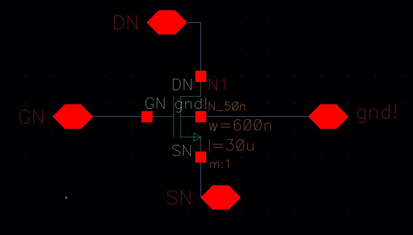 Layout
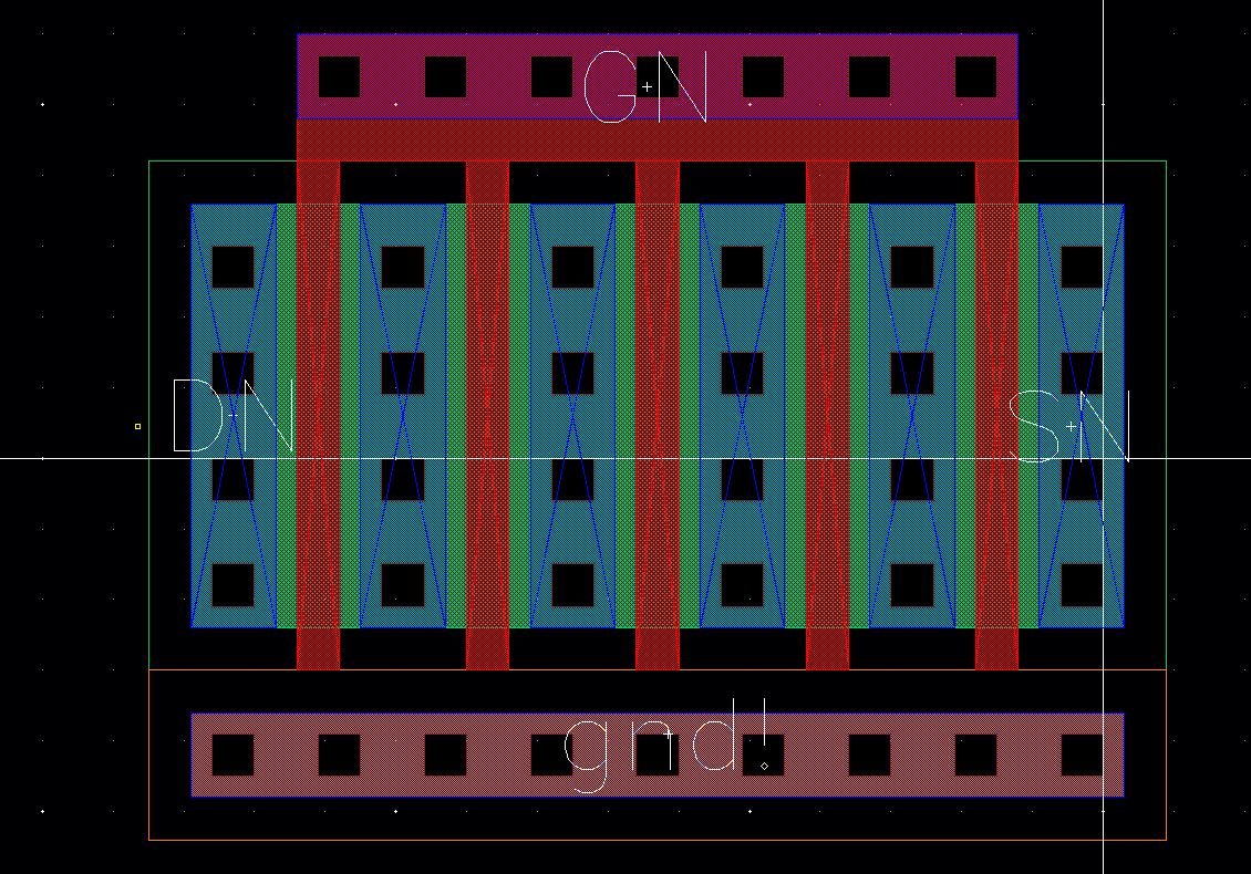
- 30u/0.6u PMOS (4 pins, DP, GP, SP, and BP)
Schematic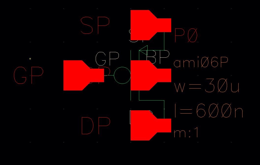 Layout
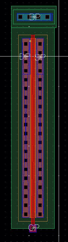
- Inverter made using 30u/0.6u NMOS and 60u/0.6u PMOS (3 pins, in, out, VDD_inv)
schematic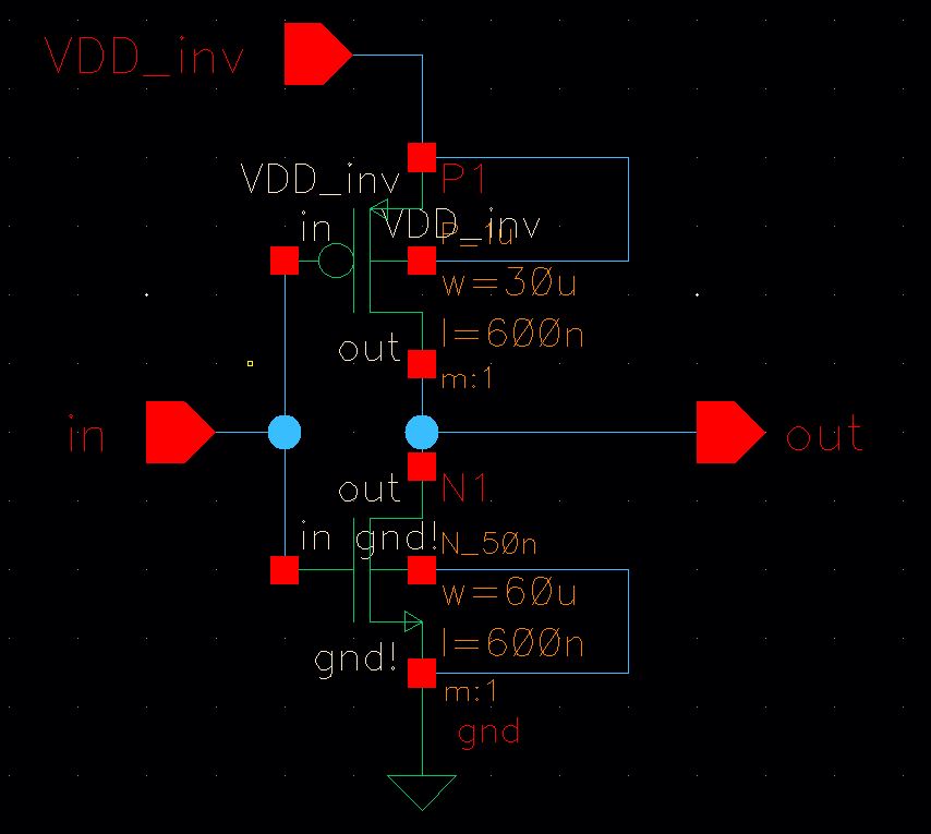 layout
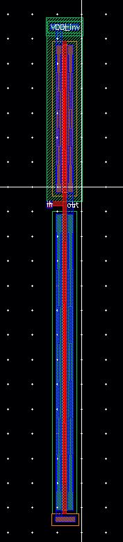
- 61 stage ring oscillator using 6u/0.6u MOSFETs with off-chip buffer (2 pins, VDD_osc and Ocs_out. Ground connected to pin 20)
Schematic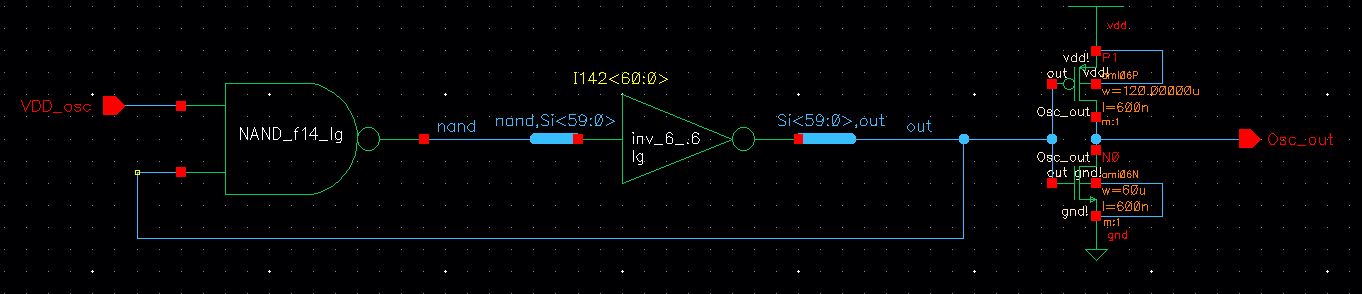 layout
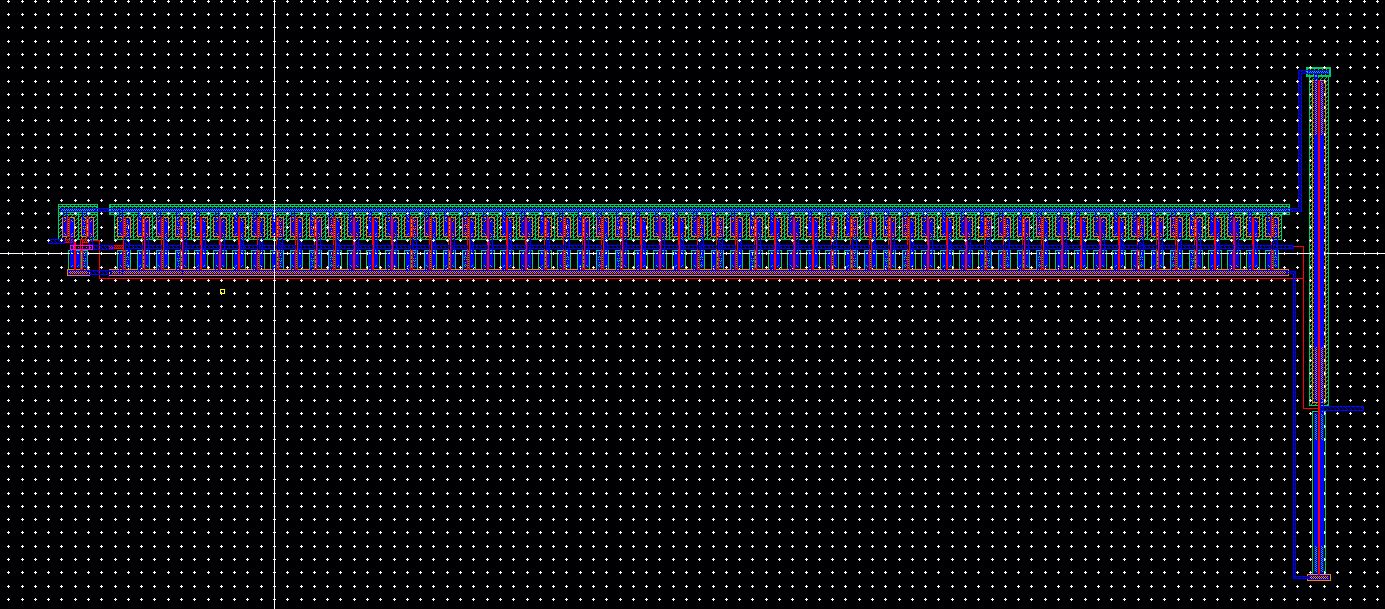
- 20k n-well resistor (2 pins)
Schematic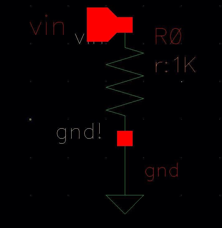 Layout
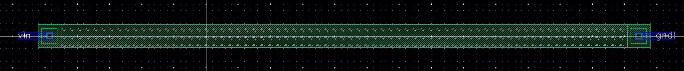
- 20k hi-res poly resistor (2 pins)
Schematic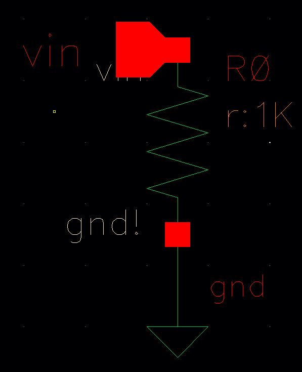 Layout
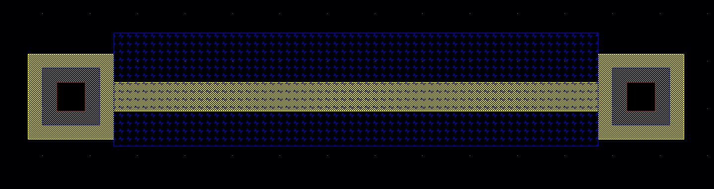 Layout
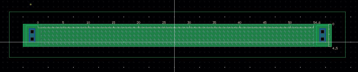
- 1k
p+ resistor (3 pins, need n-well to isolate the p+ from the p-substrate
and the n-well needs to be tied to a voltage >= either side of the
resistor)
Layout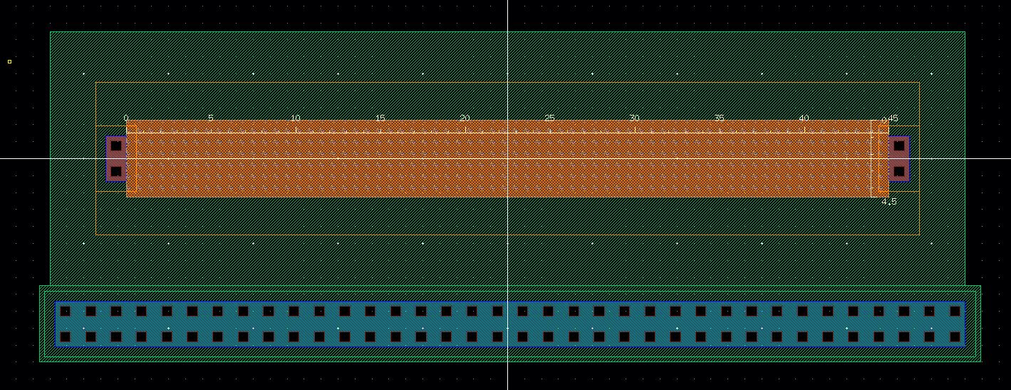
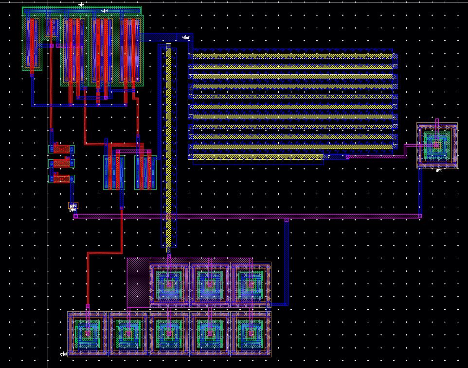
- Bandgap reference (2 pins, VDD_bg and Vref)
Schematic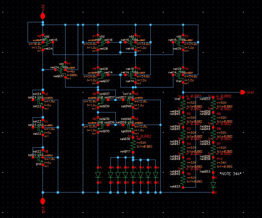
Layout
Part I: Layout
Final Schematic
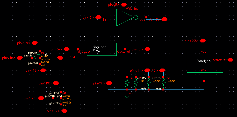
In
order to LVS, the N+ and P+ resistors must be excluded. They will still
be in the layout, but Cadence is unable to identify them (even with
R_id).
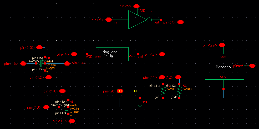
Schematic for LVS
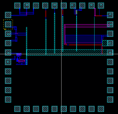
Final Layout
LVS
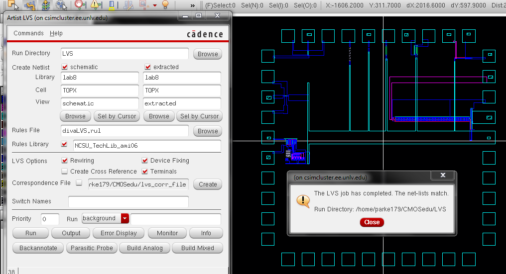
Now that the layout matches the schematic the chip is ready to be sent off for testing.
Final Chip: MOSIS_ChipXX
Part II: Testing
When fabricated chip comes in the components need to be checked seperately to ensure that the design fuctions properly.
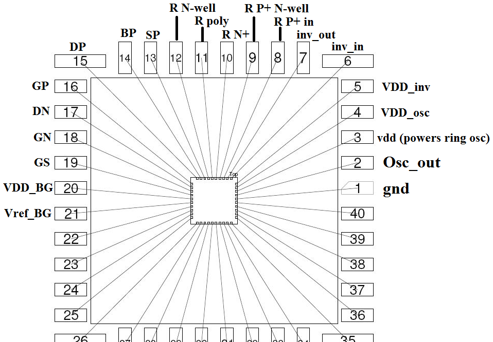
- 30u/0.6u NMOS (3 pins, DN, GN, SN)
| Pin | Connected to | Reads |
| DN | 5V (VDD) | |
| GN | 0V | |
| SN | | 5V |
- 30u/0.6u PMOS (4 pins, DP, GP, SP, and BP)
| Pin | Connected to | Reads |
| DP | | 5V -> 0V |
| GP | 0V -> 5V | |
| SP | 5V | |
| BP | 5V | |
- Inverter made using 30u/0.6u NMOS and 60u/0.6u PMOS (3 pins, in, out, VDD_inv)
| Pin | Connected to | Reads |
| In | 0V->5V | |
| Out | | 5V ->0V |
| Vdd_inv | 5V | |
- 61 stage ring oscillator using 6u/0.6u MOSFETs with off-chip buffer (2 pins, VDD_osc and Ocs_out. Ground connected to pin 20)
| Pin | Connected to | Reads |
| VDD_osc | 5V | |
| Osc_out | | Frequency |
- 20k n-well resistor, 20k hi-res poly resistor, 1k n+ resistor (2 pins)
Measure the resistance between both ends, resistance should be close to what is in the layout- 1k
p+ resistor (3 pins, need n-well to isolate the p+ from the p-substrate
and the n-well needs to be tied to a voltage >= either side of the
resistor)
Connect the n well to 5V and then measure the resistance between the remaining pins.
- Bandgap reference (2 pins, VDD_bg and Vref)
| Pin | Connected to | Reads |
| VDD_bg | 5V | |
| Vref | | 1.25V |
Creating backups
Dropbox was used to backup all screenshots, project files, and html files. I
do so by using the dropbox folder as my active work area to save to,
and then dropbox automatically uploads changes to the files.
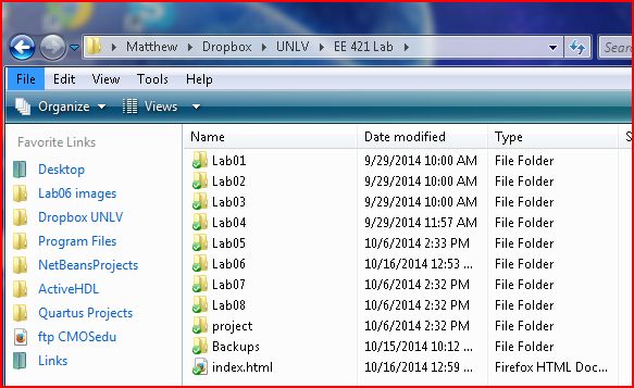
Download Lab8 Directory
Group Members' course directories:
Matthew Parker
Tiny Yu
Leanna Guevara