EE
421L ALU Project Design:
Schematic Implementation
Authored
By Alan Fortes
on November 9, 2014
fortesa@unlv.nevada.edu
The
lab directory cells are found ALUproj_af_f14.zip
Part 1: Design goals and considerations
The purpose of this project is to create an 8 bit ALU that has the following functions:
Bitwise ANDing of a pair of 8 bit words.
Bitwise ORing of a pair of 8 bit words.
Bitwise addition of a pair of 8 bit words.
Bitwise subtraction of a pair of 8 bit words.
The selection of the desired function will be guided by two input bits, F0 and F1.
For the sake of simplification and dichotomization, we will use the following configuration for our ALU:
| F1 | F0 | Function |
| Logic | 0 | 0 | AND |
| 0 | 1 | OR |
| Math | 1 | 0 | Add |
| 1 | 1 | Subtract |
Notice
the split between the logic and math functions, where our logic
functions have F1 bits of 0 and our math functions have F1 bits of
1.
This will allow us to split our ALU into two main branches: The
logic and math branches. The logic branch part of the ALU will output
logic
functions, and the math part will output math functions to our ultimate
output of Z. Both of these branches will be connected to a
2 to 1,
8 bit mux. The signal being fed to the selecter of this mux will be
connected to the F1 bit. If the F1 bit is a 0, the the output will be
a logic function from our logic branch. If the F1 bit is a 1, then the output will be a math function from our math branch.
Regarding
the F0 bit, this bit will be used to select which function each branch
will transmit to the mux that decides which function type the user
would
like to be displayed. If F0 is a 0, the logic branch will transmit the
result of bitwise ANDing A and B. If F0 is 1, the logic branch will
transmit the bitwise or of the two words.
For
the math branch, if F0 is 0, addition will be performed and transmitted
to the mux. If F0 is 1, then subtraction will be done and sent to the
mux.
The mux the two branches are connected to act as the gate keeper regarding which branch is to be displayed.
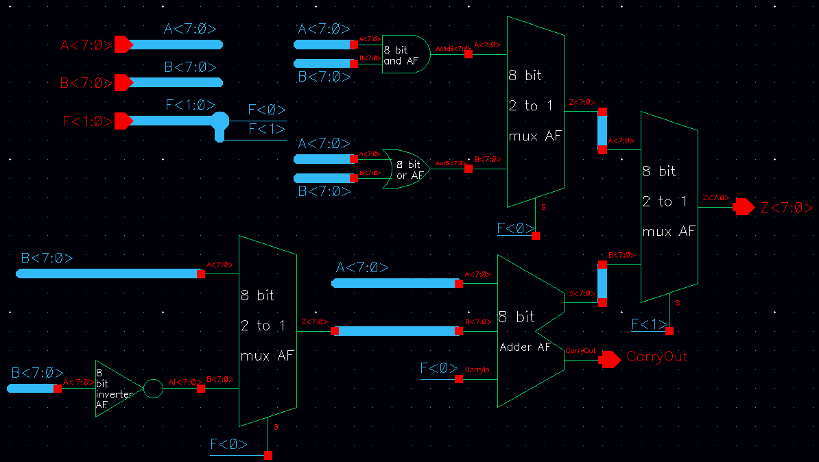
Part 2: Implementing the design in a schematic
The
creation of our ALU will use various previously created gates and
digital logic devices. This includes, 8 bit and gates, or gates,
inververters, and muxes.
These digital logic structures are capable of being found in lab 7.
As previously mentioned, our ALU will begin a mux connected to two branches. The logic branch will have a mux to decide which logic function to
output.
The math branch will have to control whether or not subtraction will be
done. This will be determined with a mux receiving an original value
of
B, and a two compliment value of B. If subtraction is requested, then
the inverted value of B is fed through the mux to the 8 bit adder, and
a high
signal is sent to the Cin part of the adder to account for the addition of 1 bit into the process. Here is the result:

Here
is the symbol of the ALU. Although the ALU has an output for Carryout,
this will not be used, since we are dealing strictly with an 8 bit ALU.


Part 3: Testing the ALU for proper output.
Here
is the general testing schematic for the ALU. The inputs for A and B
are radomly chosen pulses to ensure maximum reliability of whatever is
thrown at the ALU.
The only thing that will vary for this schematic
will be the function. To easily access the output vector waveforms,
simply double click the spectre state of the desired
cell view's simulation

To easily
access the output vector waveforms seen below, simply double click the
spectre state of the desired cell view's simulation cell.

Here
is the testing of bit wise AND. Our input is 10011101 for A and
10100110 for B. The result should be 10000100. The output matches.

Here
is the testing of bit wise OR. Our input is 00000011 for A and 1100100 for B. The result should be 11001011. The output matches.

Here
is the testing of Addition. Our input is 01100110 for A and 01111000 for B. The result should be 11011110. The output matches.

Here
is the testing of subtraction. Our input is 11111101 for A and 10010011 for B. The result should be 0. The output matches.

In order to ensure that my lab is lost forever, I back up my work by emailing it to myself.


EE
421L ALU Project Design:
Layout Implementation
Part 1: Design goals and considerations
Now that the schematic has been created and verified to work correctly, the actual layout of the chip will be made.
In order to demonstrate the analogous components, and to ensure that it is easy to see that the ALU has been implemented
correctly, the first step to be taken is create the layouts of the individual compnents of the ALU, as seen below:
This means that there will be a layout of each block in the schematic.
There will be an 8 bit layout of an and gate, or gate, 3 muxes, an
inverter, and an adder.
These 8 bit components will then be connected appropriately to create the final goal of an 8 bit ALU.
Part 2: Laying out individual components
Here is the layout of an 8 bit AND gate.

Here is the layout of an 8 bit OR gate.

Here is the layout of an 8 bit MUX.

Here is the layout of an 8 bit Inverter.

Here is the layout of an 8 bit Adder.

Here is a close up of an individual adder of the 8 bit adder.

Part 3: The final product
The
final product of putting these together is an 8 bit ALU. The vertical
strips of metal 1 sticking out at the top are the input for the ALU.
Input of the 8 bits of A are the left and
the
8 bits for B are at the right. The horizontal strips of metal 2 and 3
are used disseminating the inputs of A and B to the appropriate parts
of the 8 bit components.
The vertical strips of metal 3 at the bottom are the outputs, Z. The Function controls are the small
strips of poly right above the strips of metal 2 near the bottom.

Here is the lvs for the layout proving that the layout matches the previously made schematic.

To ensure that my lab is not lost forever, I back up my project and report.


