Lab 6 - EE 421L
Authored
by Henry Chan,
chanh6@unlv.nevada.edu
20 October 2014
This lab is meant to design, layout, and simulate a CMOS NAND gate, XOR gate, and Full-Adder.
We
start by first creating the necessary schematics for the 2-input NAND
gate, and 2-input XOR gate using 6u/0.6u MOSFETs (both NMOS and PMOS).
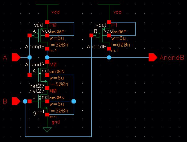
2-Input NAND Gate
Schematic:
The
schematic was created using nmos4 and pmos4 instances from the
NCSU_Analog_Parts library. The lengths and widths of the mosfets were
adjusted and the connections were made as shown below.
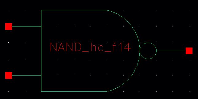
Symbol:
A symbol was created using Create->Cellview->From Cellview as shown below.
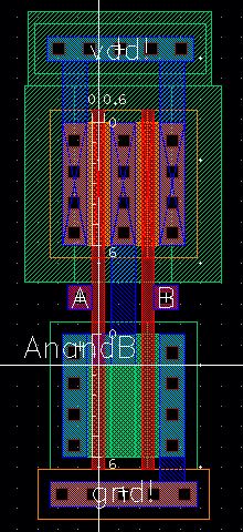
Layout:
The
layout was created using nmos and pmos instances from the
NCSU_TechLib_ami06 library. Ntap and ptap cells were included to tie
Vdd and ground sources. Pins were then assigned to the appropriate
areas for a successful LVS.
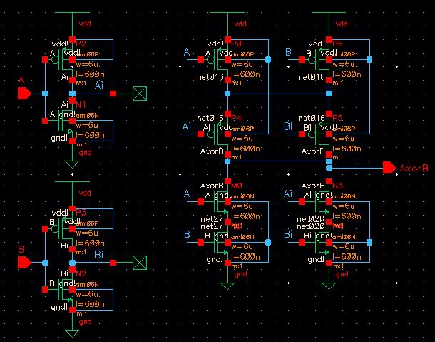
2-Input XOR Gate
Schematic:
Again, instances of nmos4 and pmos4 from the NCSU_Analog_Parts library were used to create the xor schematic.
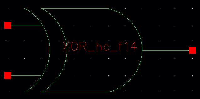
Symbol:
The symbol for the xor gate was made using the same method for the nand gate.
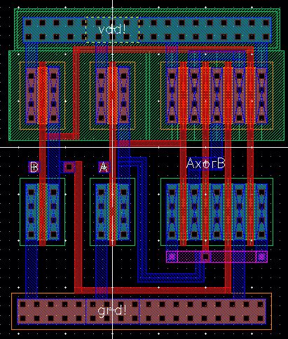
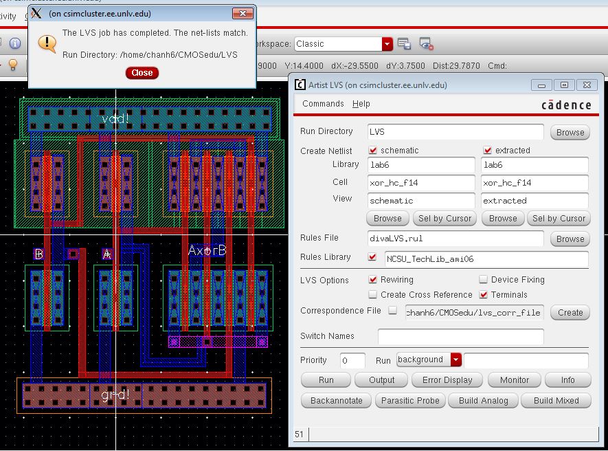
Layout:
The layout used nmos and pmos instances from the NCSU_TechLib_ami06 library.
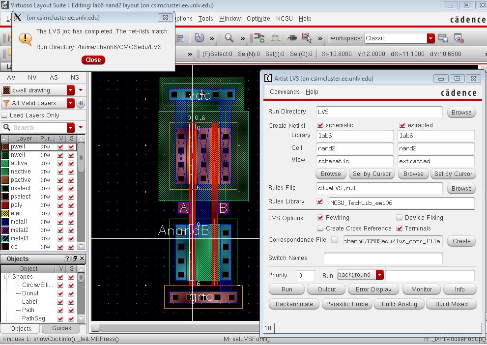
LVS shows net lists match with no errors.
Simulating the Gates
Spectre was used to simulate the logical operation of the gates for all four possible inputs (00,01,10,11).
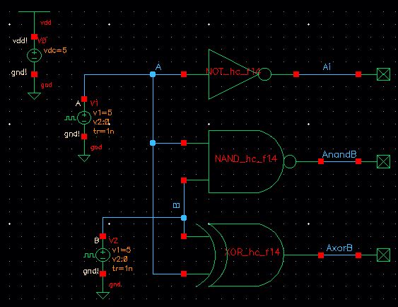
The plot below shows the correct output logic.
| A | B | AND | XOR | NOT A |
| 0 | 0 | 0 | 0 | 1 |
| 0 | 1 | 0 | 1 | 1 |
| 1 | 0 | 0 | 1 | 0 |
| 1 | 1 | 1 | 0 | 0 |
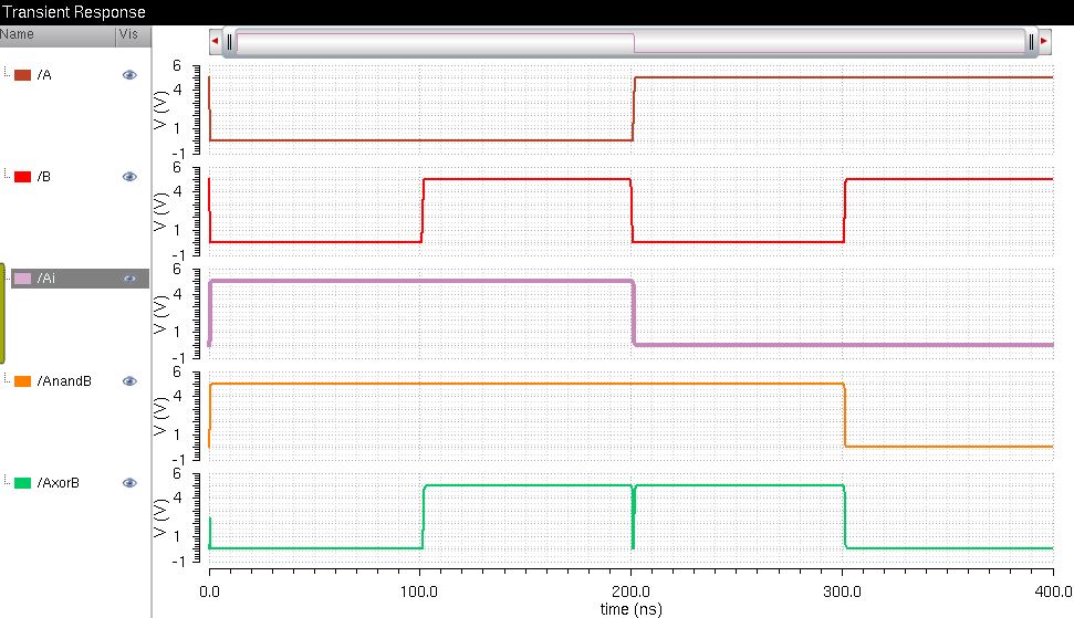
It
is important to note that any delays from one input of the circuit can
drastically affect the output results due to unsynchronized operation
of the inputs. For example, if input A must traverse through a greater
length mosfet than input B, input A may experience more delay, thus the
output may incorrectly evaluate the state of input B versus an
unarrived input A.
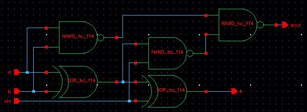
Full-Adder
Schematic:
Using the symbols from the nand and xor gates, the full-adder schematic is created.
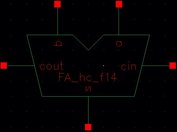
Symbol:
The symbol view was created similar to the other symbols in this lab.
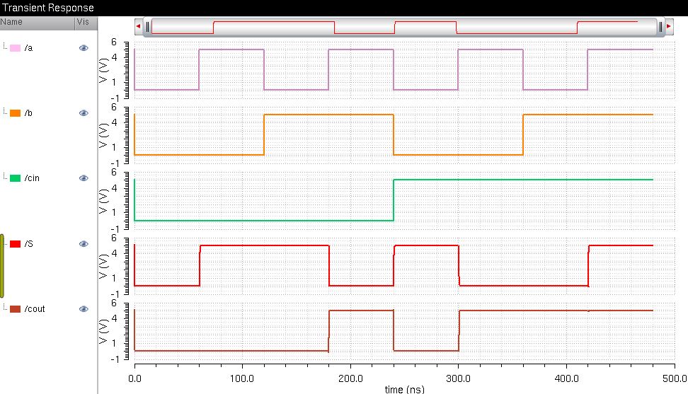
Simulation:
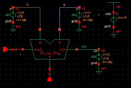
A
simulation schematic was created using the full-adder symbol above.
Three voltage pulse sources were used as inputs a,b, and cin. Each
pulse source has a different frequency in order to demonstrate all
input possibilities.
| a | b | cin | s | cout |
| 0 | 0 | 0 | 0 | 0 |
| 1 | 0 | 0 | 1 | 0 |
| 0 | 1 | 0 | 1 | 0 |
| 1 | 1 | 0 | 0 | 1 |
| 0 | 0 | 1 | 1 | 0 |
| 1 | 0 | 1 | 0 | 1 |
| 0 | 1 | 1 | 0 | 1 |
| 1 | 1 | 1 | 1 | 1 |
The simulation output shows the correct operation.
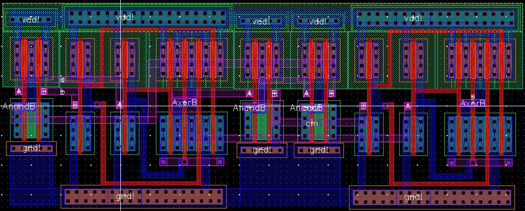
Layout:
The layout of the full-adder was created using instances of the nand and xor layouts made previously in this lab.
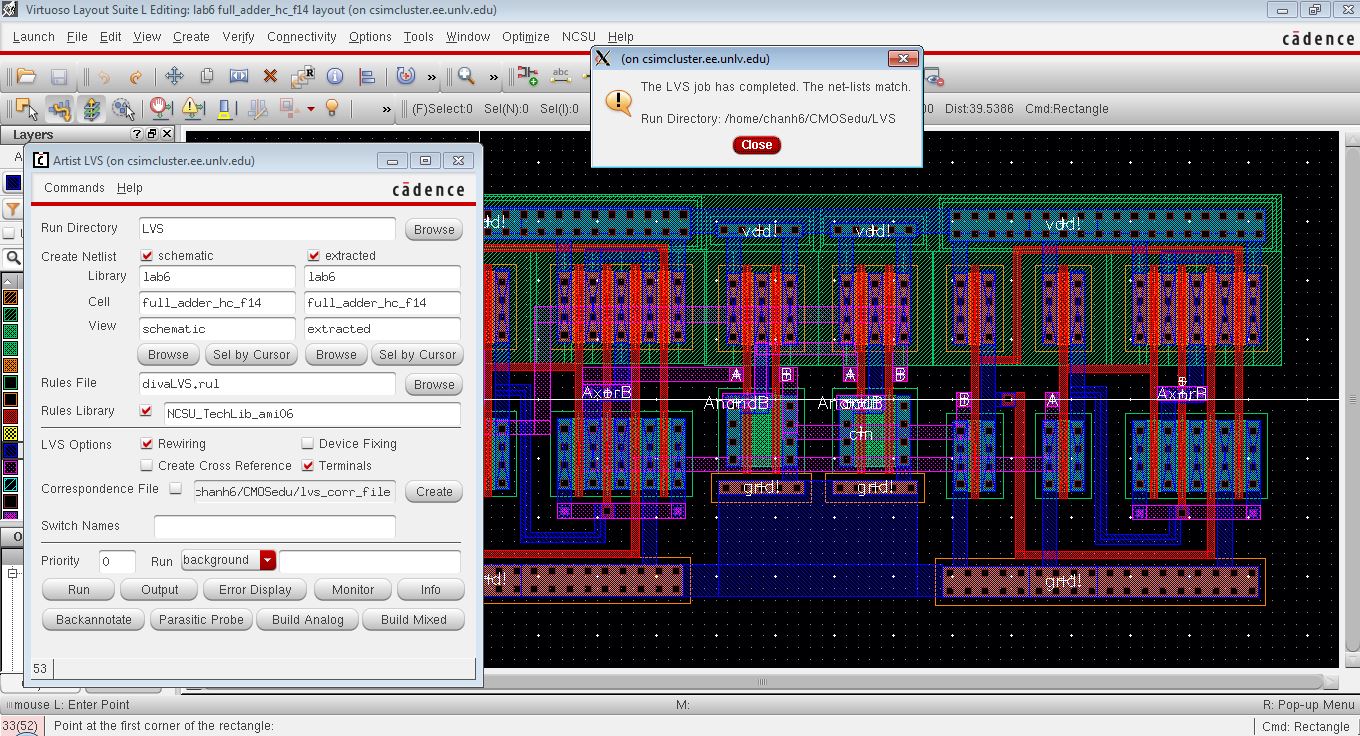
LVS shows matching netlists and no errors.
This concludes the lab, all files from this lab can be found here.
Backups of this lab were stored in a cloud service.
Return to EE 421 Labs