
Lab 7 - EE 421L
This is my 4bit Inverter and symbol: dont forget to use busses and to turn on the value for I0 so that it shows up like below or it will DRC and you will get an error. Also make sure you use input and output pin for the inverter to correctly label it when you create a symbol from it.


This is my simulation of the bit inverter to test if it was correct. I used loads 100f,500f, and 1p and a pulse from 0-5 volts.

This was my grpah i got from the simulation: Just for future refeerence i will have my loads with capacitors and ill have one wiht a noconnect to see if they gate is funcctioning correctly:

This is my shcematic for the 8bit inverter and the symbol for it:


As above i simulated the inverter but with 8 bits this time:

out<0> was my noconnnec load so that i could see if the inverter was functioning correctly:

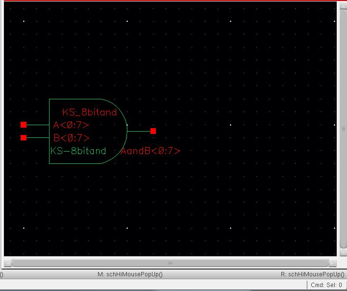
This is my 8bit nand symbol:

Then we had to simulate the 8bit nand symbol to make sure we configured it and drew the schematic properly.

Again out<0> was to make sure the gate was functioning properly:


This is my 8bit and schematic: remeber to use busses and the correct input and output pins.

Next you have to create the symbol:
Now we have to simulate the 8 bit and gate: this is my schematic i drew to test it.

Again remeber out<0> is to test the gate and then i also tested the gate with different loads.

 \
\


 next
we need to create the same procedure as above but for a mux.
First we had to create an 8 bit mux inculding the si feature and
then an 8bit mux without the si pin and using the inverter int he
schematic.
next
we need to create the same procedure as above but for a mux.
First we had to create an 8 bit mux inculding the si feature and
then an 8bit mux without the si pin and using the inverter int he
schematic.


First we had the copy the schematic into cadence. I used inverters at the outputs but if you wanted you could have used the schematic view of the inveter instead of the symbol. Which ever one is easier for you to look at when comparing the layout. As seen below this is only for the schematic of a 1bit FA. We need to make 8bits so from this you have to make a symbol then proceed to make the 8bit schematic then LVS that layout and drc that layout. But first it would be easier if you also drew the layout for the 1 bit and instantiated it 8 times intot he 8 bit then connected them with the different pins.

This is my FA symbol and FA 8but schemtic: make sure you label your wires and busses correctly alsot he pins. I found that without labeling it correctly i ran into many problems when doing my 8but layout LVS.

Then we created an 8bit symbol from the schematic:

This is my 8 bit Full Adder layout: in full view.

This is the full adder layout zoomed in: Remember to label each and and b pin as input from <0>-<7>. This is the same for the s pins but as output pins. Also remeber to create 1 cin pin in the begining and 1 cout pin at the end to match your schematic. Lastly create a pin of vdd! and ground over all 8 parts of the FA.

This is my LVS and DRC:


Lastly we need to do the same as the other gates and test our new 8bit FA using the symbol we created.

This is my output graph:

Then we have finished lab 7. These are my files:
And dont forget to back up your lab 7.

