
Lab 4 - EE 421L
Email: carpiosu@unlv.nevada.edu
In this lab we will create layouts and schematics for PMOS and NMOS transistors of different sizes. Also we will simulate our layouts and schematics to obtain the IV characteristics.
Pre-Lab
Make sure you back up all your files using the "tar -cvf backupdate.tar CMOSedu/".
Next download the tutorial 2 folder from the link in bakers website and put it in your CMOSedu folder. Dont forget to define it in your lib file so you can use the file in cadence.Then follow the tutorial.
1) first step we had to create a NMOS transistor with the width as 6u. Then make sure you create a symbol of the transistor.

2)Since we cant use the transistor for the lvs schematic because it is a 3 pin we then have to make a similiar transistor with 4pins. The 4th pin is the body and it gets tied to the ground. It should look similar to this.

Next you have to create a layout for the NMOS transsitor. Create a new cellview and instance in the nmos transistor with the width of 6u from the nscu techlib ami06.
Then add a metal1-connection-to-poly cell and a poly rectangle to connect the gate to m1_poly. Next instantiate a ptap cell in the p-substrate . Next create pins G, D, S and B. It should look similar to this.

Make sure to drc and lvs the schematic and layout to make sure there are no errors and that they match.
2.1) Next we have to create a PMOS 3 pin transistor like the nmos above. It should look like this.


2.3) Next we have to do the layout like above but for a PMOS. So instantiate the pmos layout from the same directory as above. It should look like this and make sure to make the gates G,D,S, and B. Add a metal1 poly and a poly rectangle to connect the gate to m1_poly. Next instantiate a ntap cell which connected the bulk of the pmos.

Make sure to drc and lvs the schematic and layout to make sure there are no errors and that they match.
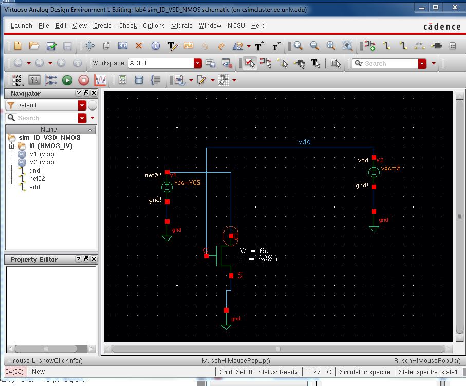
Creating the NMOS Schematic for IV Curve
First create a schematic like shown below using nmos transistor.We need to create a schematic for simulating ID v. VDS of an NMOS device for VGS varying from 0 to 5 V in 1 V steps while VDS varies from 0 to 5 V in 1 mV steps. Use a 6u/600n nmos. Make sure that you choose the vdc value to be 0. Use dc analysis. Select component parameter. Set start and stop values at 0V and 5V respectively. Change sweep type to linear and set step size to 1m.

This is the graph that you should get at the end of the sweep.

Next we need to do a a schematic for simulating ID v. VGS of an NMOS device for VDS = 100 mV where VGS varies from 0 to 2 V in 1 mV steps.
This should be your grpah if you load the state and run the output.


2)
Next we need to do the same steps as above but for PMOS.
your schematic should look like below. varying from 0 to 5 V in 1 V steps while VSD varies from 0 to 5 V in 1 mV steps.

This is the graph and how to setup the ADE.


This is my setup of the ADE and how to run it.

This is the graph output.

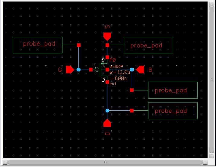
Next we needed to create a schematic of the NMOS with probe pads. It should look like below.

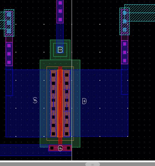
Then we need to create a layout similar to the schematic so we can LVS them.
This is a zoomed in portion. With the NMOS.

After laying out the pads and connecting the NMOS to the pads with the same pins. Make sure you LVS it to the schematic we created earlier to make sure they match.

Next we need to do the same for PMOS. This is the Pmos schematic i created below. Make sure ther width is 12u not 6.
This is what my layout looked like and i LVSed it to make sure it matched the schematic of the PMOS.

These are my files for the Files