Lab 2 - ECE 421L
Koby sugihara,
Today's
date 9/19/14
Lab
description:
To do Lab 2 we had to create N-well resistors and create our own 10k DRC.
First we had to create this schematic into our own resistors and symbol.

Then I created a library called Lab2 in cadence and made this schematic for the resistor.

Then we turned it into a symbol that looks like this:

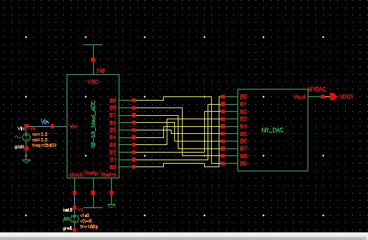
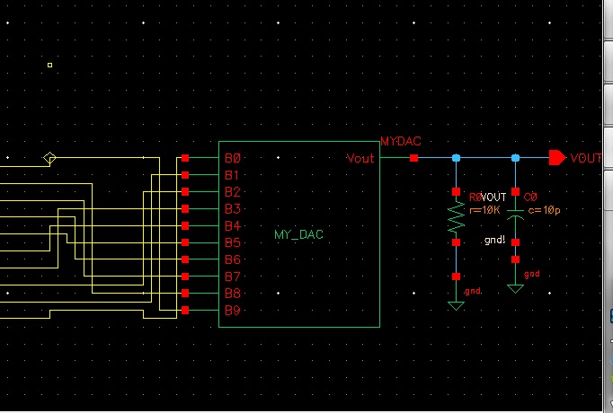
Copy the ideal
10bit _DAC and go into the schematic. Then go to the Ideal DAC and
decsend hiearchy. Then delete everything in there and put these symbols
in to follow the schematic. Connect them all top to bottom in order
from b0 to b9.

After
you finish that make sure you check and save. Now open a new schematic
int he folder and this is where you are goign to test the delay of a
10pf capacitor at vout and. Make sure you ground b0-b8. Then connect a
pulse source of 0 to 5v at the b9 node. Then connect the capacitor at
the vout parrallel to theDAC.

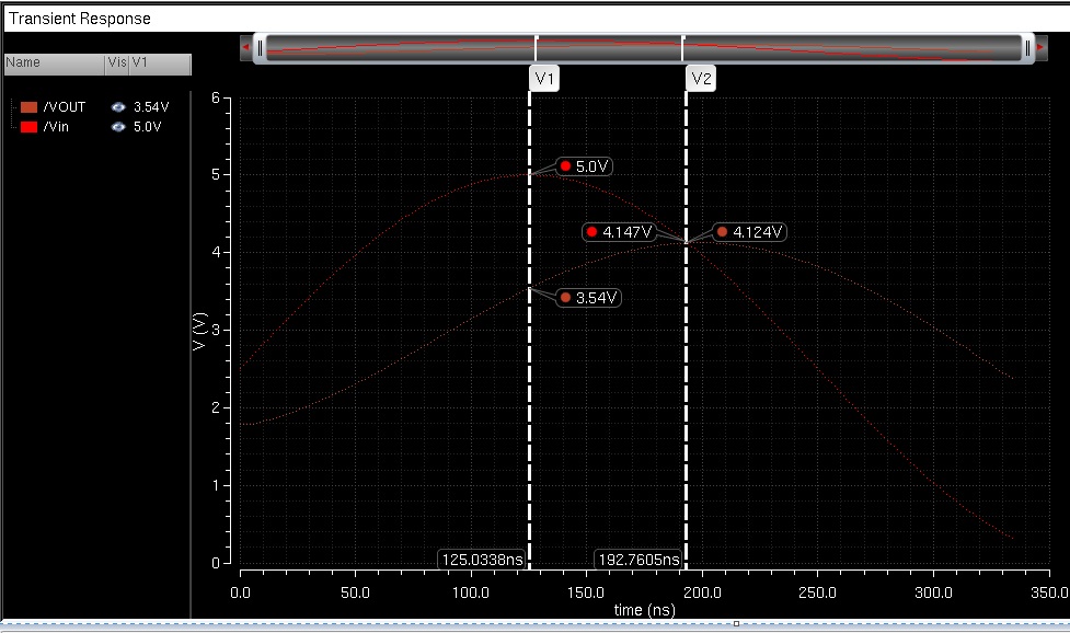
Check and save this. Then Run the ADE, and plot Vout and Vin. Also run this as a tran for 500ns. This should be your output.
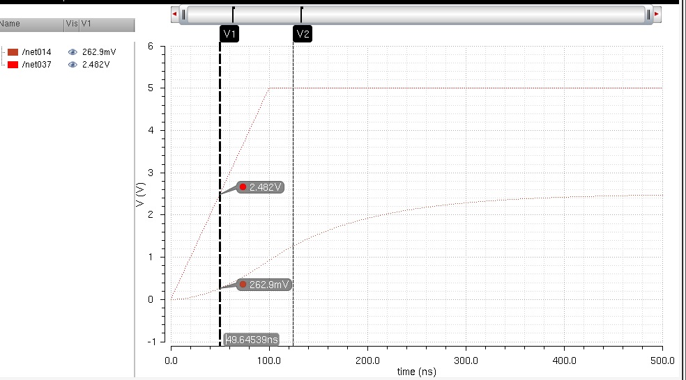
To
find the time delay you look at the time delay you look at 0.5vin and
0.5vout. Compare the times by subtracting 124ns-50ns=74ns.
To hand calculate to check your answer you can use this formula:0.7RC. So you would get 0.7(10k)(10X10^-12) and you should get 70ns. Which is close to our simulated answer.
Next copy ideal ADC_DAC. Replace the DAC that is there with your DAC you created.
sim to make sure it works and you should get this.
To
determine the output resistance, we calculate the parallel and series
resistance of each and you should get 2R || 2R = R. For the last bit we
have 2R instead of R thus it becomes 2R || 2R = R again.
Next we can start creating a 10k load ont he end of your output parallel to your DAC. It should look like this.
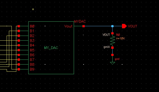
After
you put the resistor into the load check and save and run your
schematic in the ADE. Load the state and run it as a tran, for 1u.
 You
should get vout to be half of vin because 10k parallel with 10k
resistor becomes a voltage divider and divides into half of the
voltage. (2.5v)
You
should get vout to be half of vin because 10k parallel with 10k
resistor becomes a voltage divider and divides into half of the
voltage. (2.5v)
Next you can change thet output load to a capacitor. (10pf)
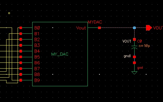
Run
the simulation at tran 400n and you should get this graph. You can
calculate the time delay by subtracting the delays form the graphs.
And as before byhand you can calculate the delay by 0.7RC.
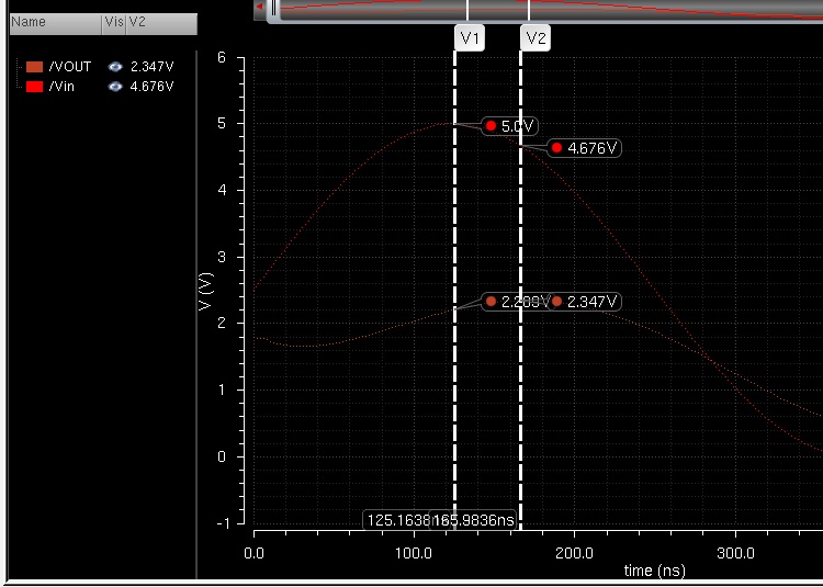
Lastly you have to put a RC load of 10k=R and 10pf=C. It should look like this then sim it:
After the simulation the graph should look like this:
If
the resistance switches are not small compared to R then it can affect
the delay time heavily and draw less current to the circuit.
Return to EE 421L Labs