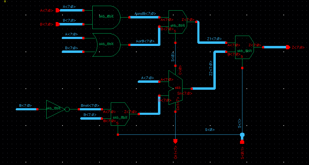
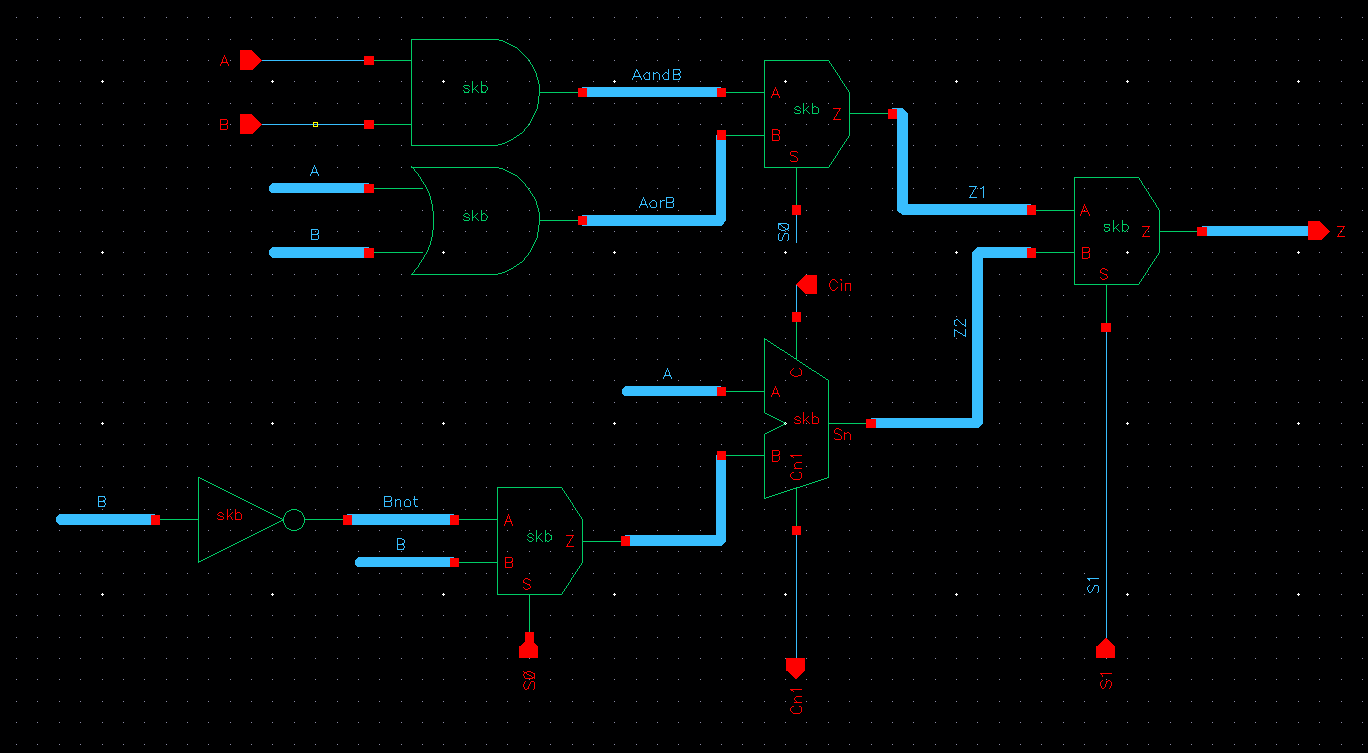
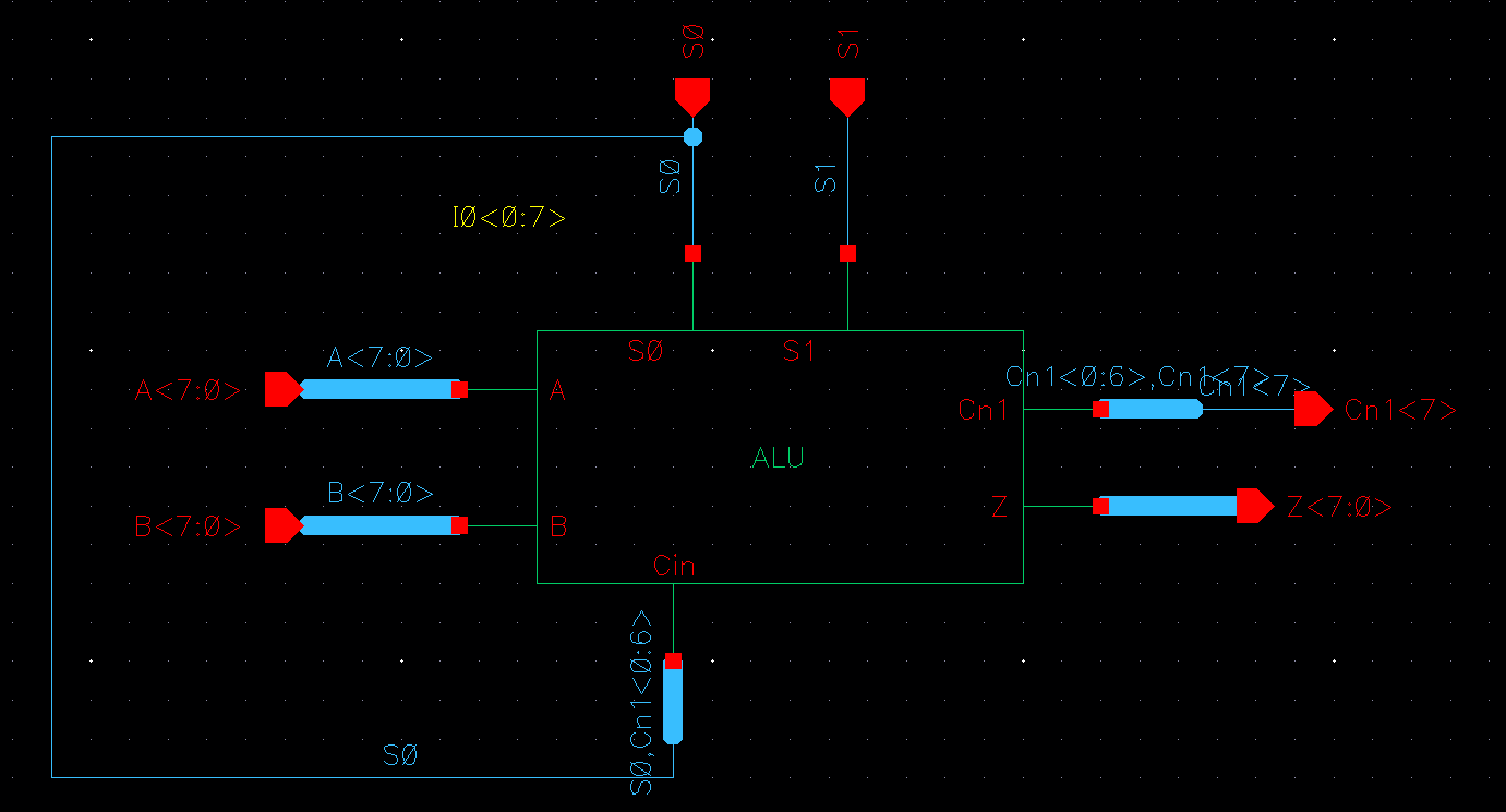
Project - ECE 421L 

Authored by: Stephen Berta - 2000138373

(bertas@unlv.nevada.edu)

11/08/14 

SCHEMATIC

Project: We are to build an ALU (Arithmetic Logic Unit)  with 4 basic functions: Add, Subtract, And and Or. We will be doing this for all 8 bits for this lab, this design will utilize previously built schematics and symbols to build our design. The design was straight forward and as expected considering we have covered labs on each independently however the subtraction was not entirely straightforward. Since a computer does not subtract the traditional way we must resort to 2's complement (to effectively add a negative number).  We will accomplish this by inverting our B signal based on what the transmitted signal is. For instance if we want to do subtraction we will choose that S0 is equal to 1 allowing the inverted B to be chosen allowing A and B prime to be added, then the S0 (still 1) is fed into the FA as a 1 creating our carry in letting us have the full 2's complement.

http://cmosedu.com/jbaker/courses/ee421L/f14/students/bertas/proj/ALU%20SCHEMATIC.PNG

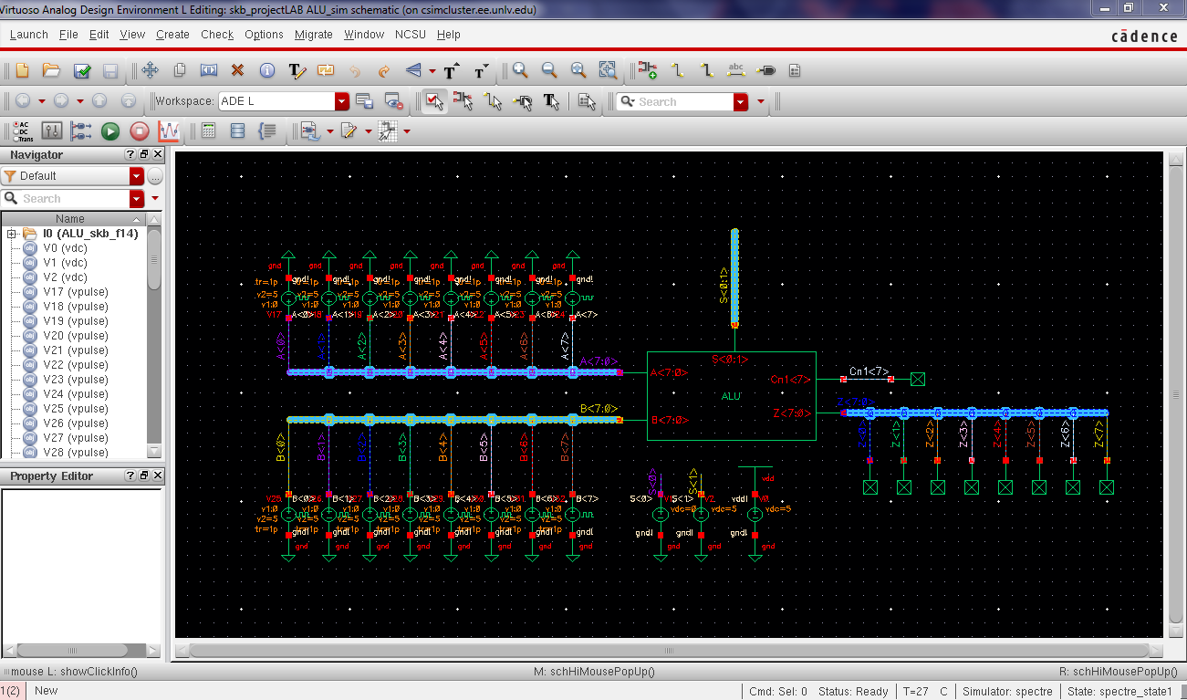
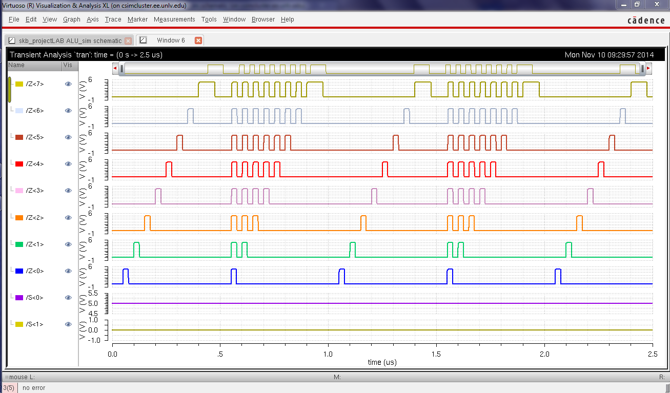
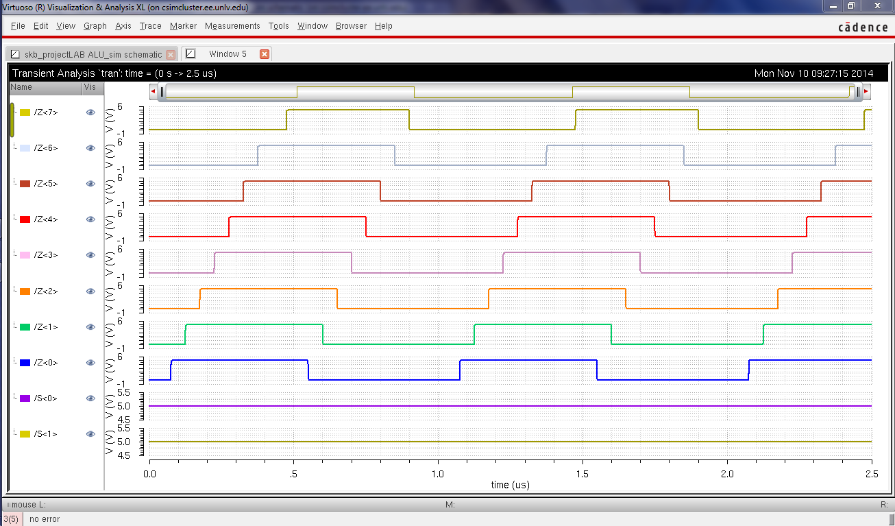
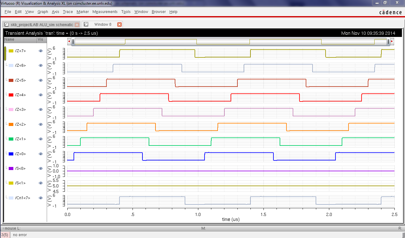
Below we can see the simulations for the above schematic. Keep in mind that S<0> and S<1> are the following for the following functions: 00 Addition, 01 Substraction, 10 OR and 11 AND.

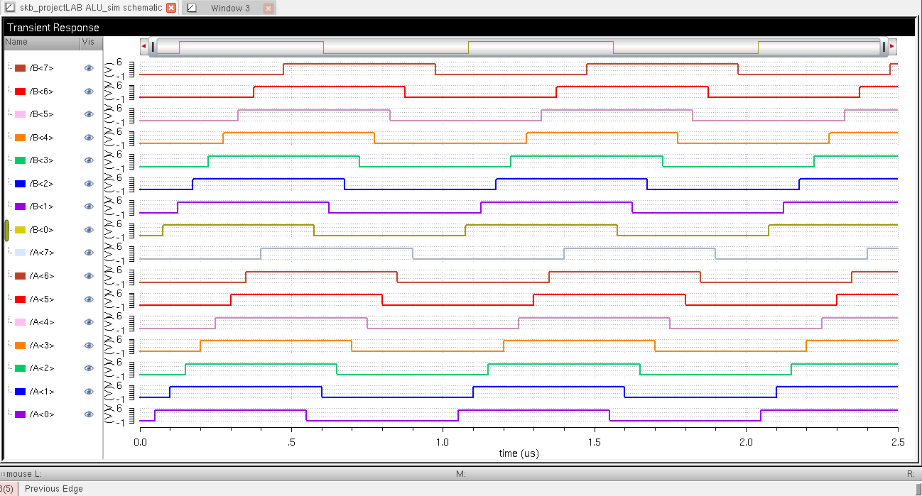
Below are the results using an A input with a 50nS delay (adding 50n per bit) and B using a 75nS delay (adding 50n per bit). First are the same inputs that i used for everything followed by the results.

http://cmosedu.com/jbaker/courses/ee421L/f14/students/bertas/proj/Schematic.PNG

Input:

http://cmosedu.com/jbaker/courses/ee421L/f14/students/bertas/proj/ALU%20Input.PNG

00 Results (addition)

http://cmosedu.com/jbaker/courses/ee421L/f14/students/bertas/proj/00%20result.PNG

10 Results (or)

http://cmosedu.com/jbaker/courses/ee421L/f14/students/bertas/proj/10%20result.PNG

11 Results (and)

http://cmosedu.com/jbaker/courses/ee421L/f14/students/bertas/proj/11%20result.PNG

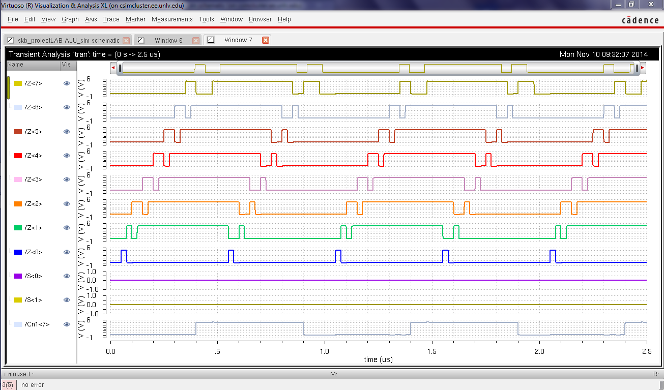
01 Results (subtraction)

http://cmosedu.com/jbaker/courses/ee421L/f14/students/bertas/proj/01%20result.PNG

LAYOUT

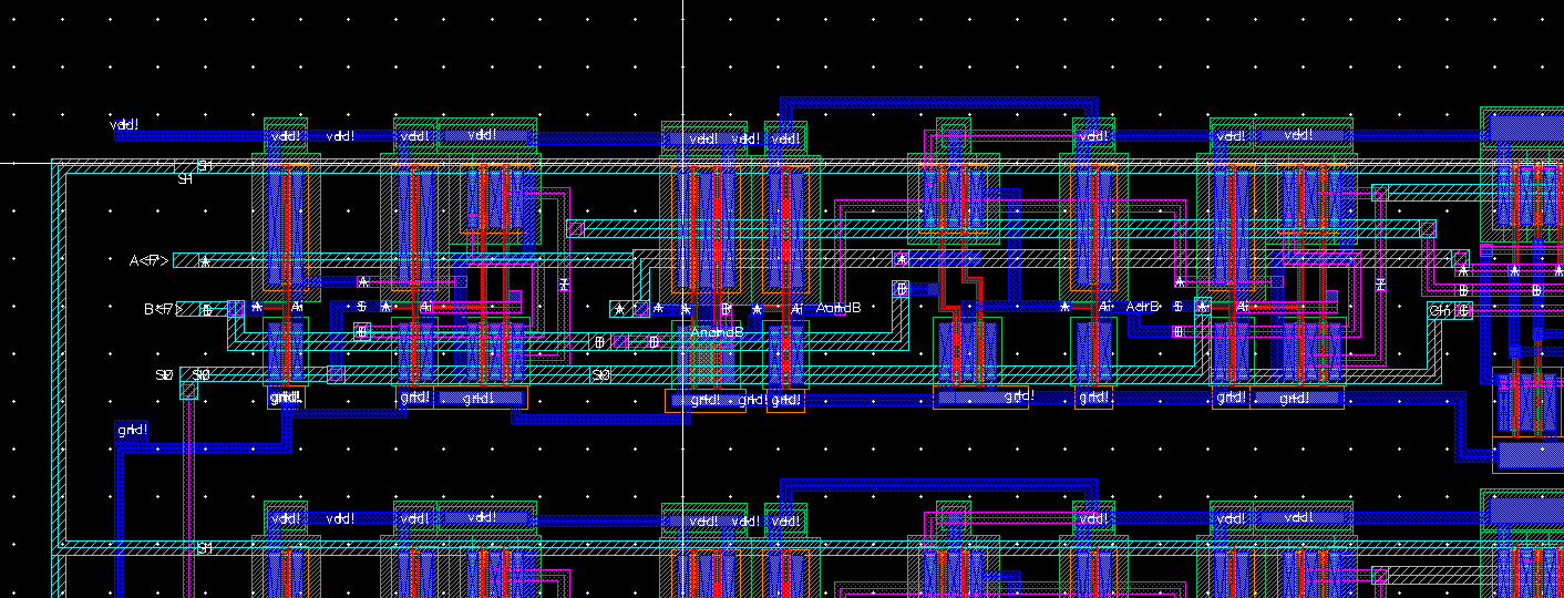
For the layout of the 8 bit ALU I decided it would be best to layout a 1 bit first and then copy it 8 times. This would minimize my work as the only connections that would need to be made outside of the block (1 bit block) would be the input/output connections instead of having to repeat the same connections between muxes/gates etc. (if I were to use the 8 bit gate schematics). Using this idea I laid out the other gates that we would be using and set off to build a 1 bit ALU. First I used the previous 8 bit schematic and simply knocked off the bracketed input terms (A<7:0> becomes A) thus making it a 1 bit. I also realized the need for bringing in a Cin bit terminal for the full adder during subtraction mode since this bit would be cascaded down much as the 8 bit Full Adder was.

http://cmosedu.com/jbaker/courses/ee421L/f14/students/bertas/proj/1bit%20schematic.PNG

Next up I began to layout the ALU using my newly made one bit gates.

http://cmosedu.com/jbaker/courses/ee421L/f14/students/bertas/proj/1bit%20lvs.PNG

After this was complete I began to work on the final 8 bit schematic/layout by simply copying this with 8 instances and creating a schematic much like that of the full adder (allowing the cascade use of the Cout bit  or Cn1 in my schematic).

http://cmosedu.com/jbaker/courses/ee421L/f14/students/bertas/proj/8bit%20schematic.PNG

And the layout:

http://cmosedu.com/jbaker/courses/ee421L/f14/students/bertas/proj/Overall%20View.PNG

http://cmosedu.com/jbaker/courses/ee421L/f14/students/bertas/proj/LVS.PNG

A snip showing the S0 connection followed by the cascading nature of the design:

http://cmosedu.com/jbaker/courses/ee421L/f14/students/bertas/proj/S0%20Connection.PNG

http://cmosedu.com/jbaker/courses/ee421L/f14/students/bertas/proj/Cascaded%20Couts.PNG

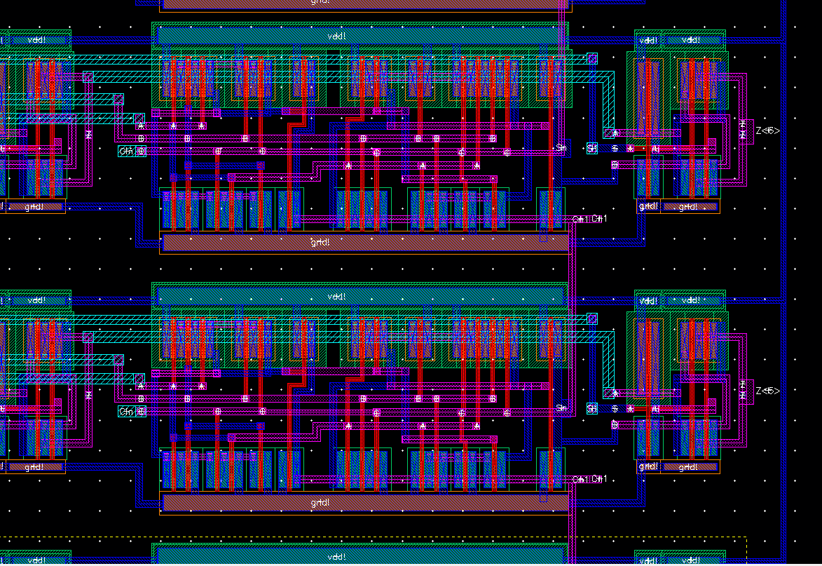
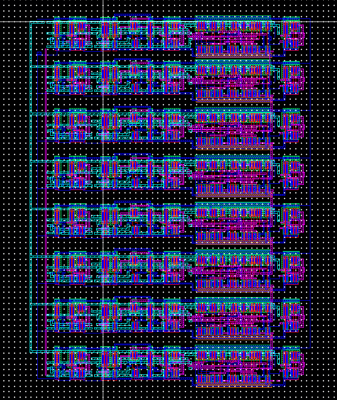
And an overall view showing all the connections with the stop level set to 0 to show the use of 8 identical blocks and identical connections with the exception of the first/last bits.

http://cmosedu.com/jbaker/courses/ee421L/f14/students/bertas/proj/8-bit%20blocks.PNG

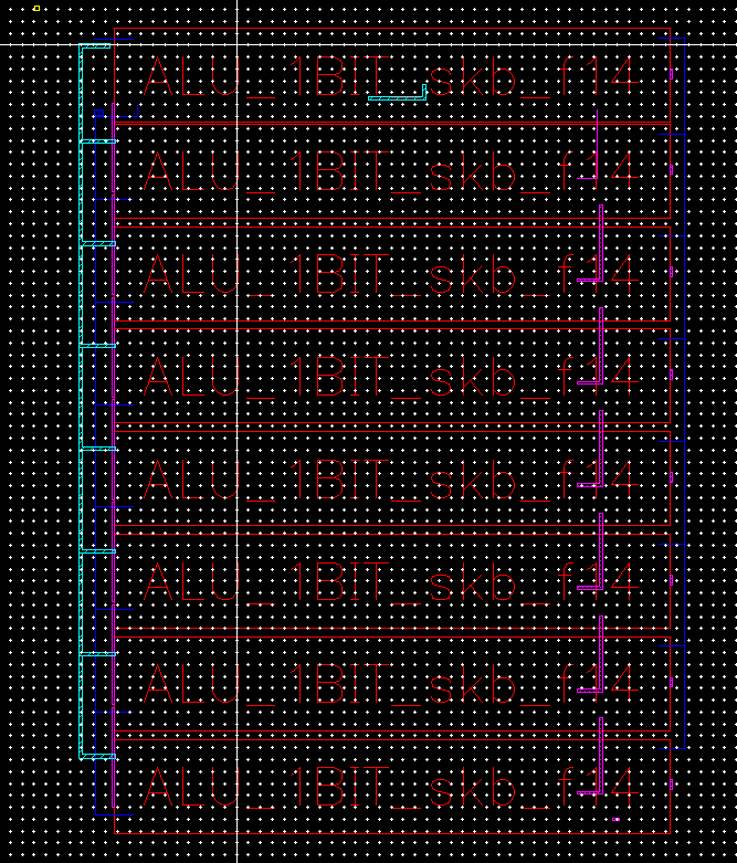
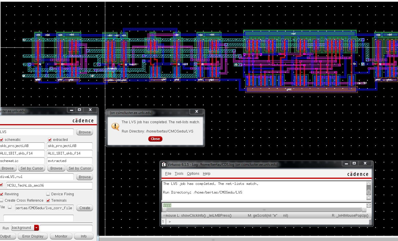
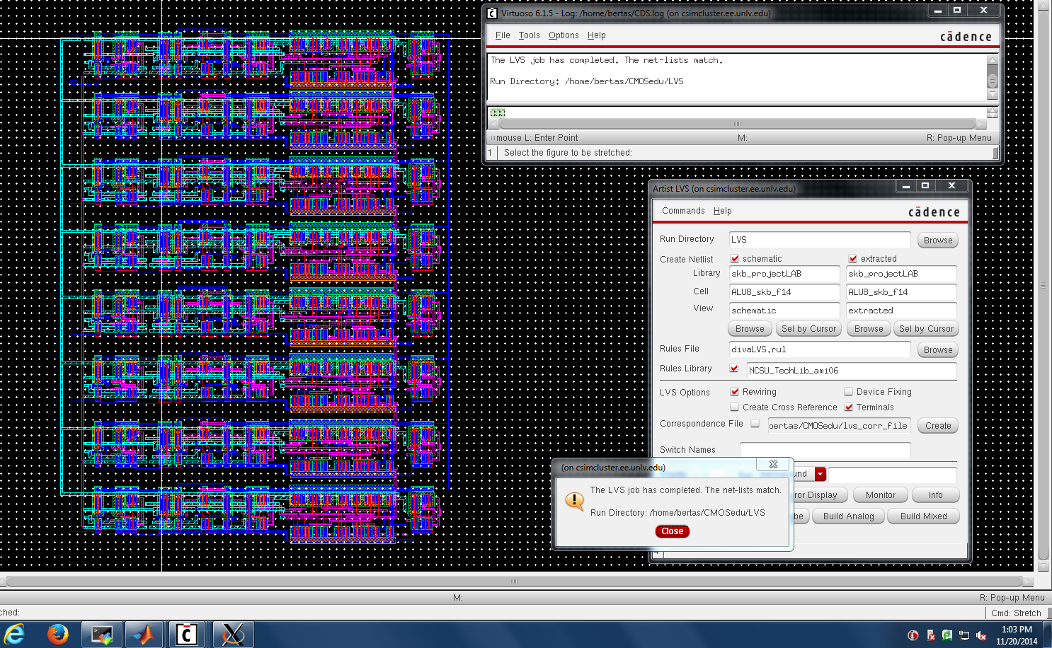
The final layout of the 8 bit ALU is labeled ALU8_skb_f14 in the design directory.

Download file directory here.

http://cmosedu.com/jbaker/courses/ee421L/f14/students/bertas/proj/backup.PNG

Return to lab folder