Lab 07 - ECE 421L
Lab 7: For this lab we initially had to use or create a 2 bit NAND, Inverter (also known as a NOT gate), NOR. Then we must create AND and NOR gates which will simply be previous designs with the addition of the inverter. After creating the 2 bit version of this we will convert them to 8 bit versions.
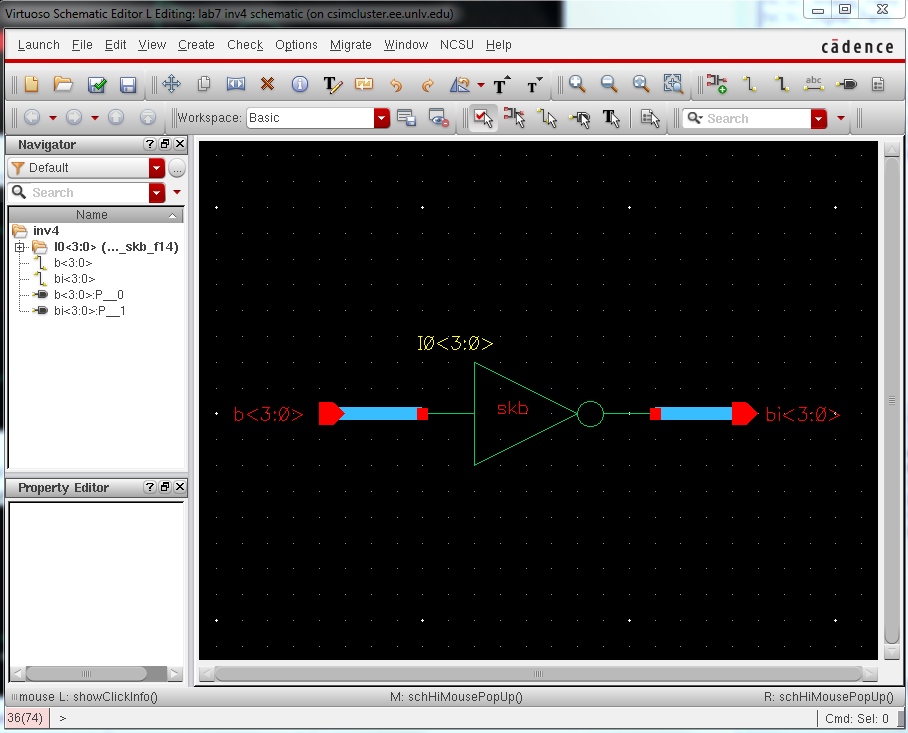
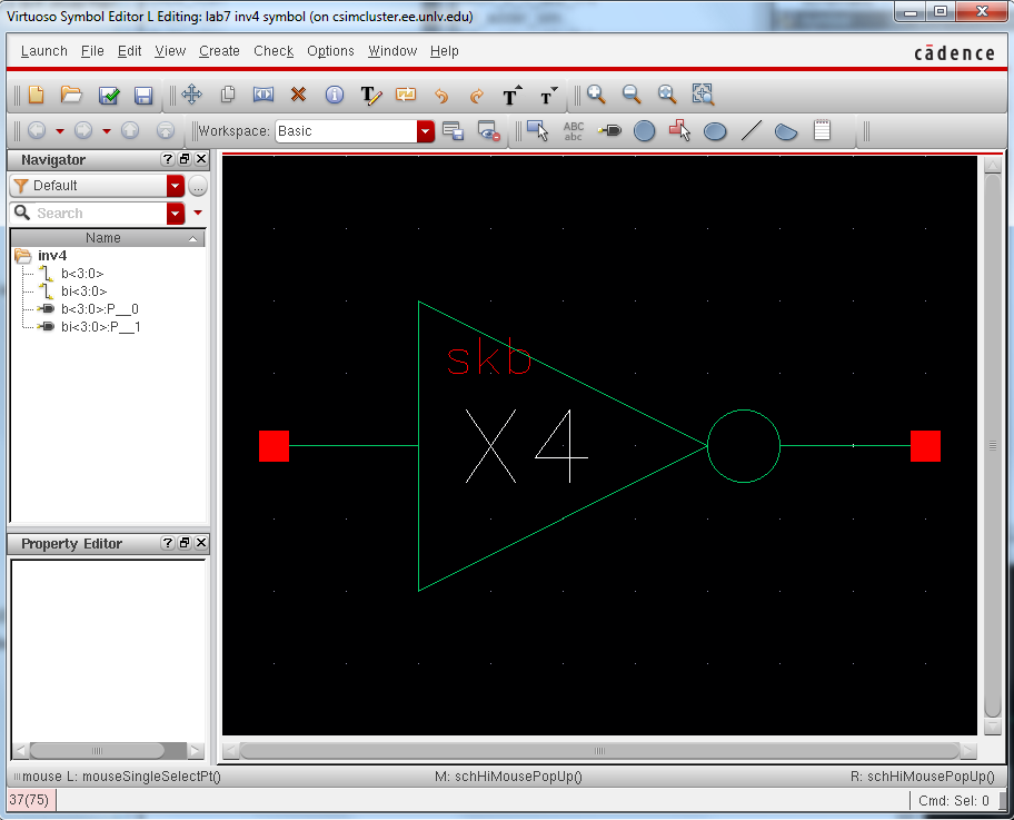
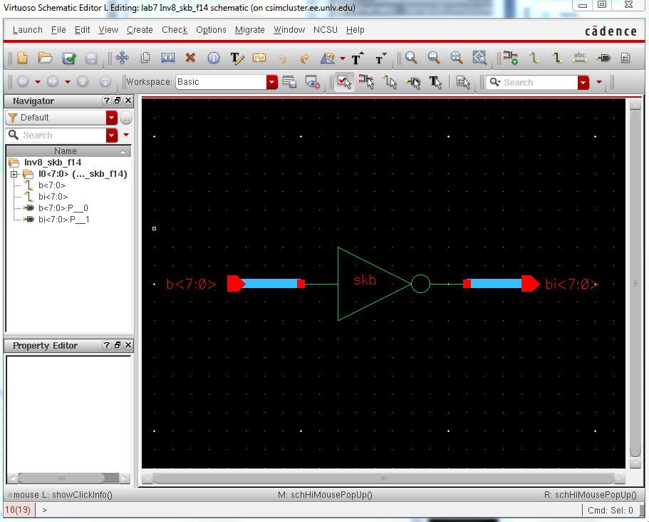
We will begin with the inverter that we previously used and place it into our 4 bit schematic. By adding the bus we are able to draw a single line to represent a group of lines (in our case below 4). We then turn this schematic into a symbol that is ready to be tested.
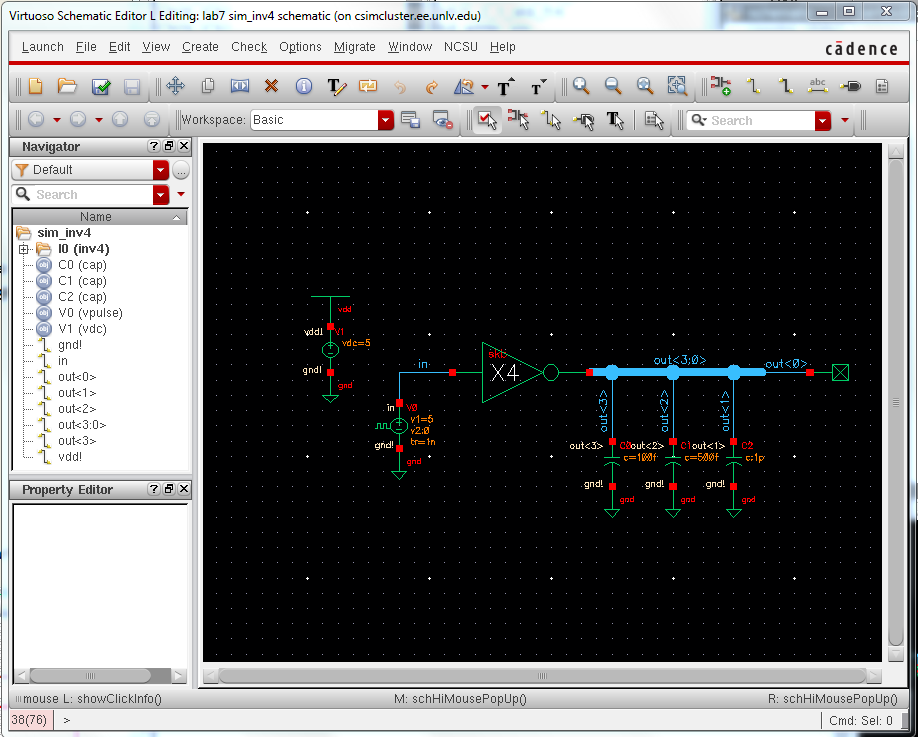
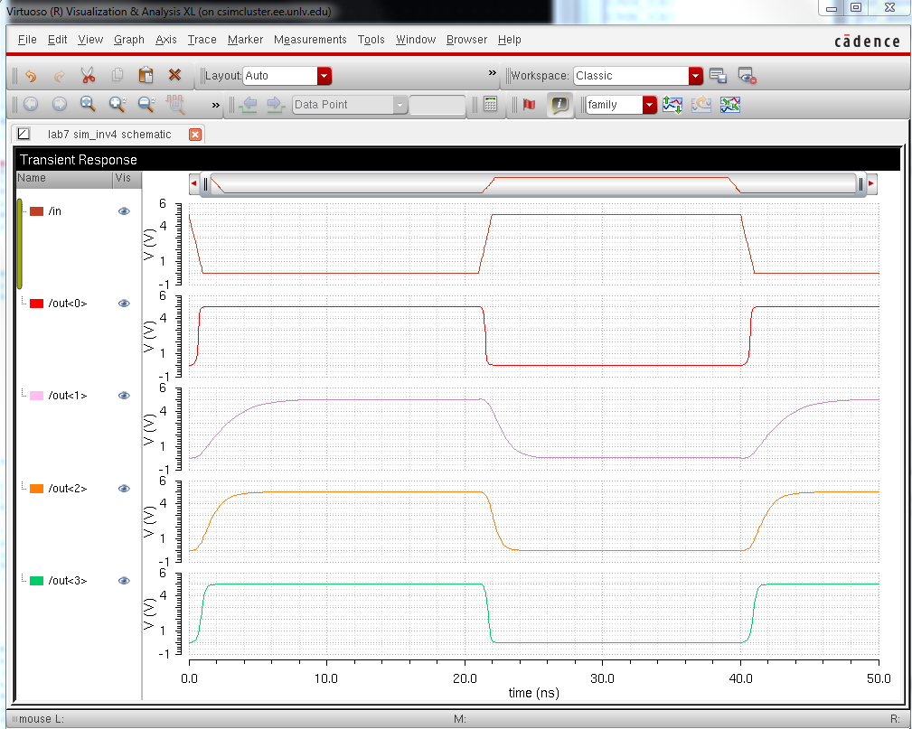
Here we can see our results and also see that it creates a small RC delay is present in our results as expected. Now that we have created and verified our 4 bit inverter we can create the 8 bit in the same fashion.
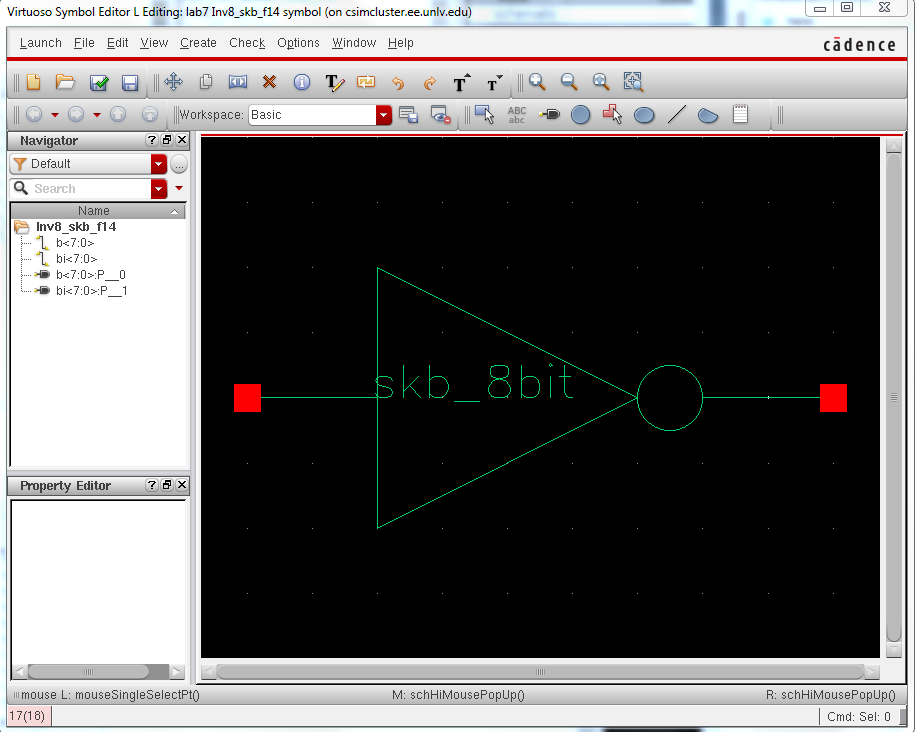
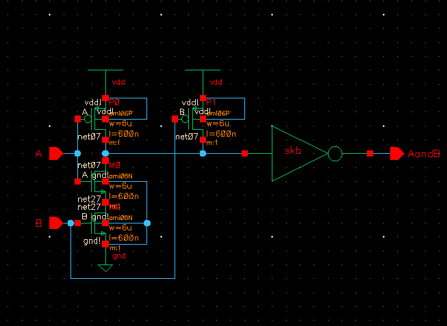
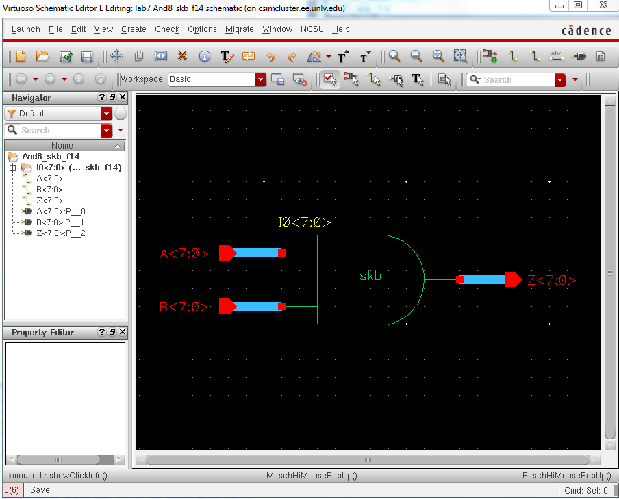
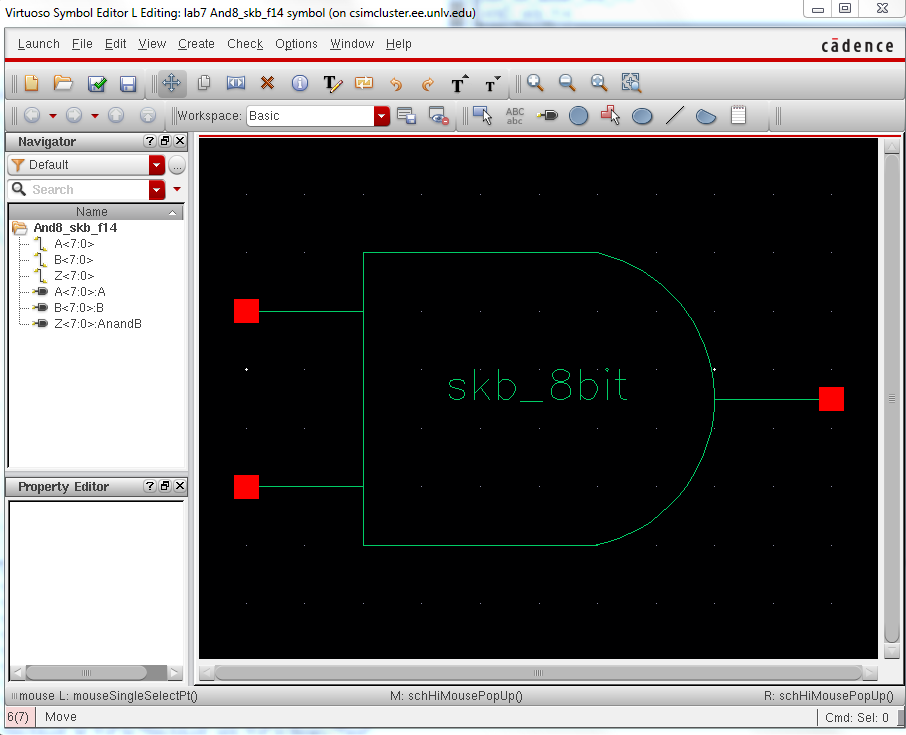
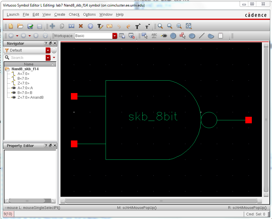
Now all we have left for the 8bit inverter is to simulate it. I will wait until I have all the gates designed and ready to go (8 bit versions) to simulate. This will allow me to test all the symbols/schematics from one central file. Now we will move onto the layout of the 8 bit AND gate. Since we covered the NAND gate last week, we will simply use that schematic and add an inverter to the end of the schematic thus giving us our AND.
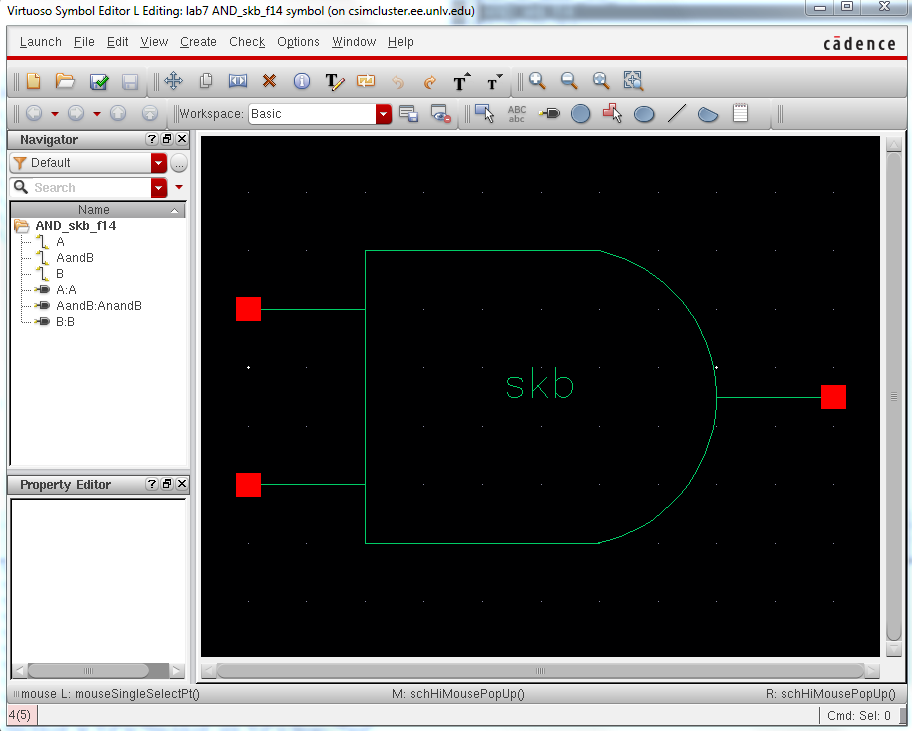
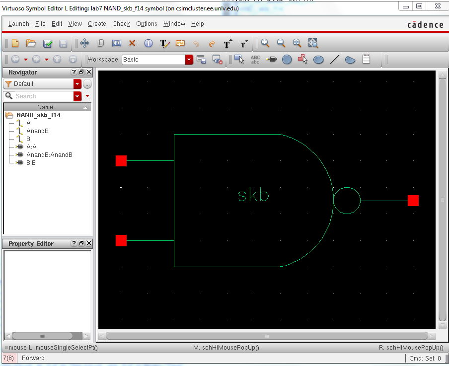
We are now ready to simulate this. We will save the symbol for later to simulate it in our master simulation file. Next, we will tackle the NAND gate using the same schematic that we used last week.
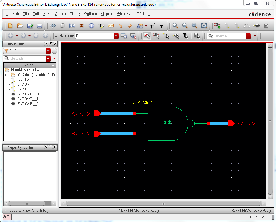
This symbol as the others will be saved for the overall simulation file. Next we will tackle the NOR gate.
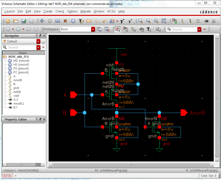

Once again this will be saved for the overall simulation.
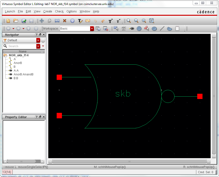
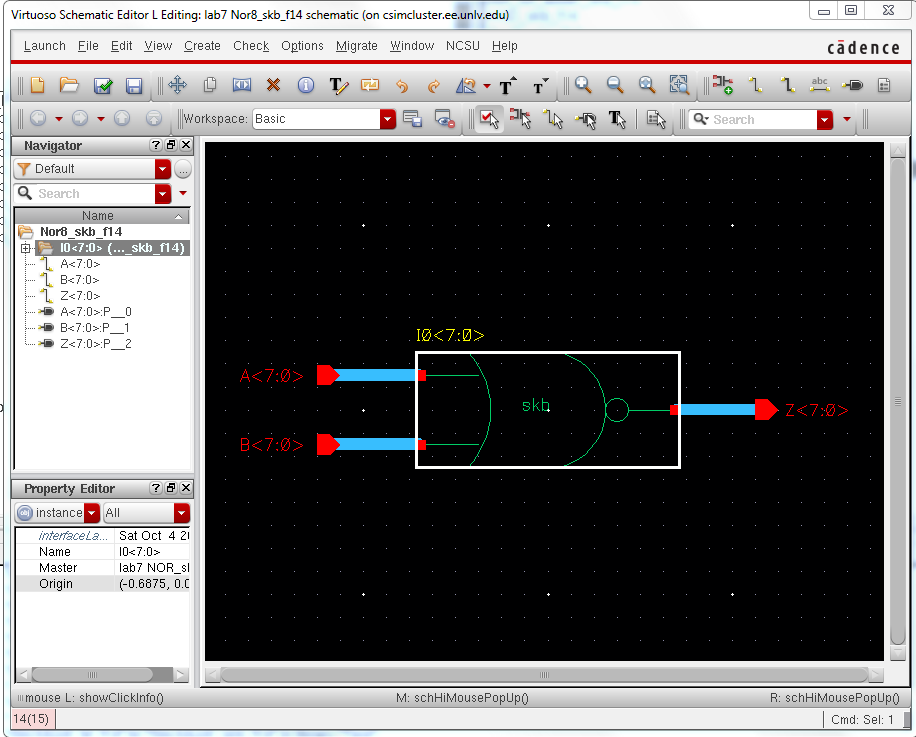
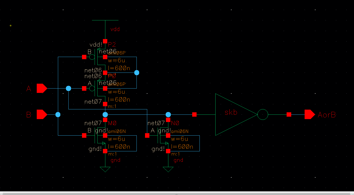
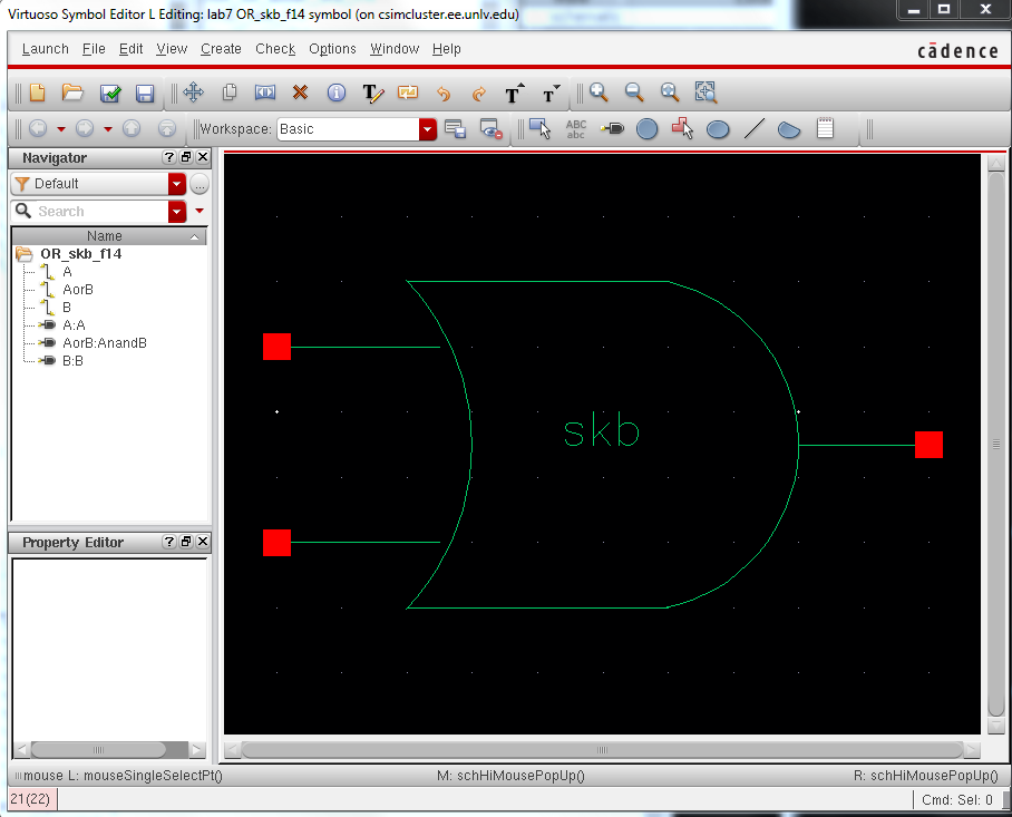
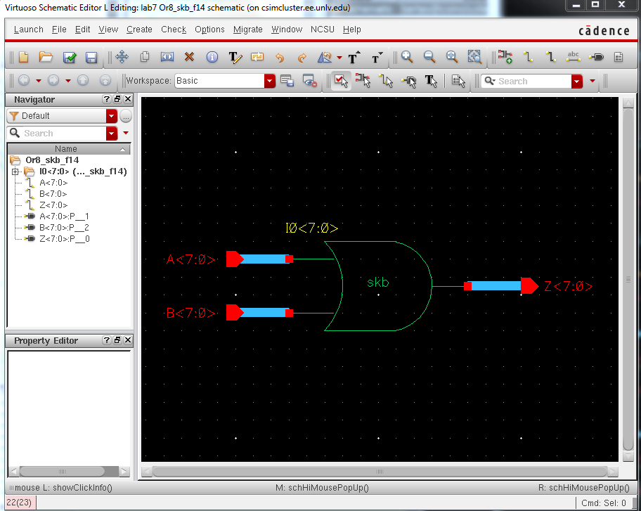
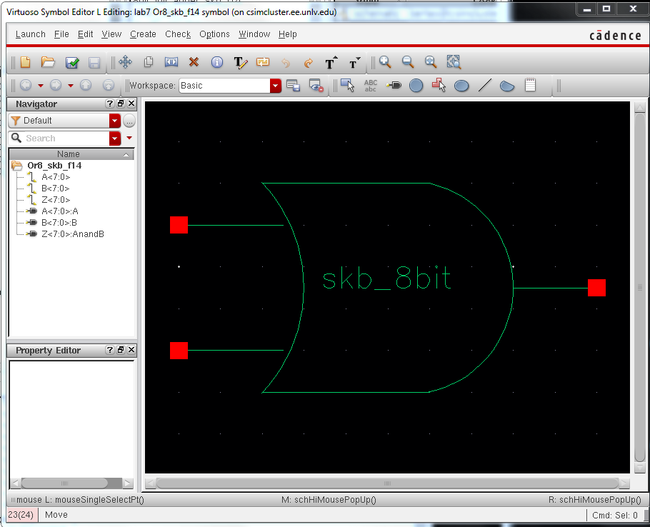
Our next gate will be an OR gate, as such we will take the same NOR schematic and simply invert the output.
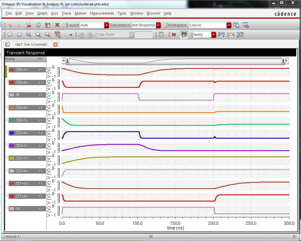
Now that we have created all our 8 bit symbols we are able to simulate the gates. For this we will run them against two differing capacitive loads (arbitrarily selected as 10p and 1p). This will create a small RC delay but will still be sufficient to allow us to test our schematics.
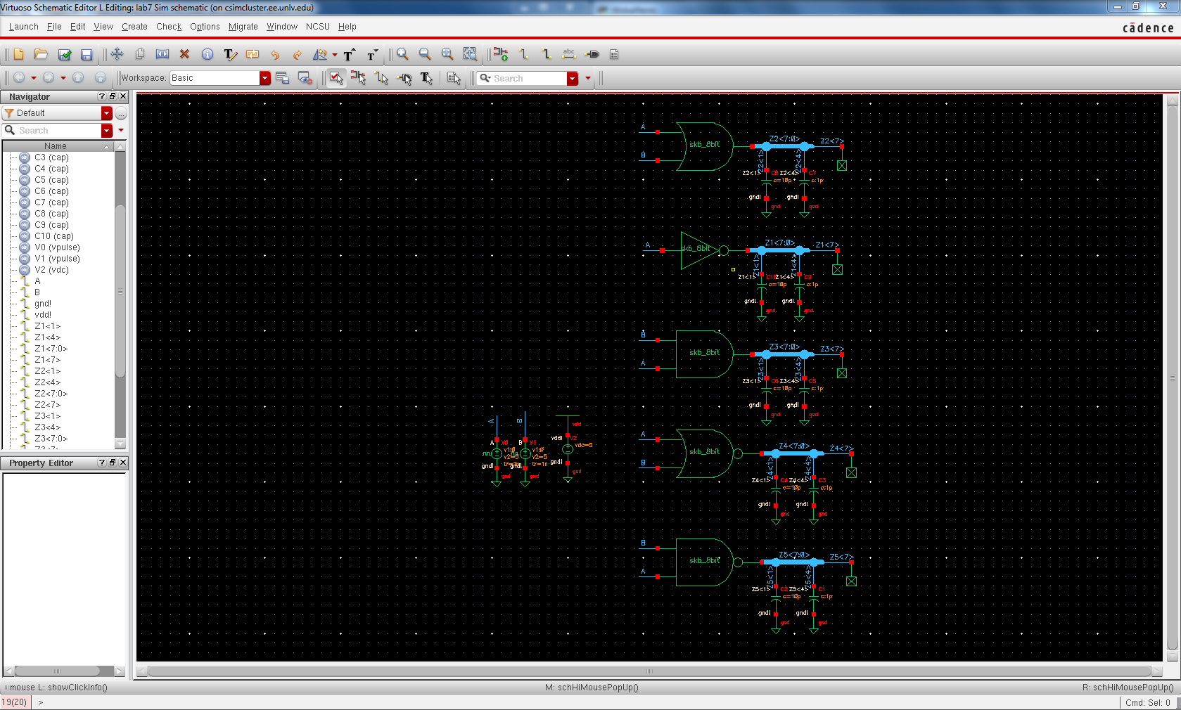
The results are then produced with our small RC delays but also we are able to see that given the inputs all our schematics run as expected.
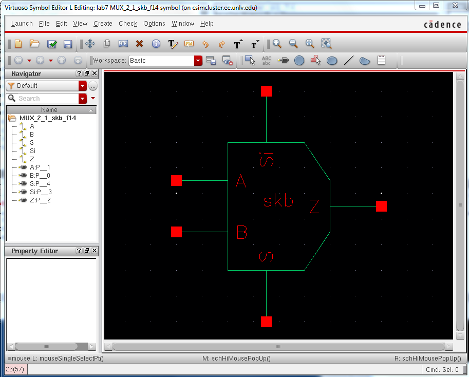
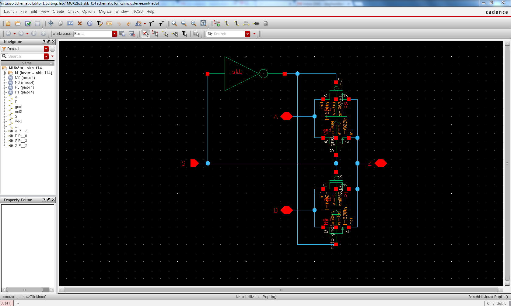
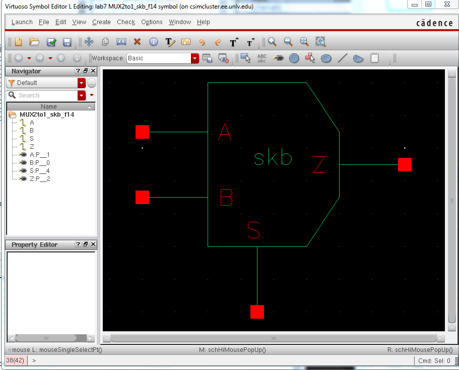
Next we are tasked with creating a 2 bit MUX. The schematic was included in the lab and is as follows.
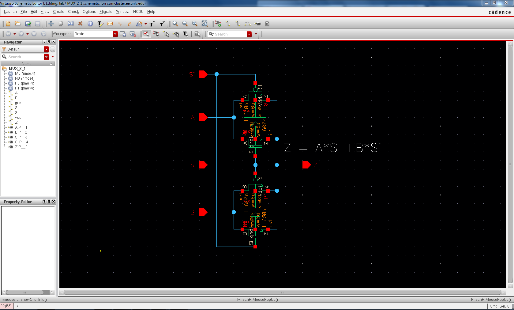
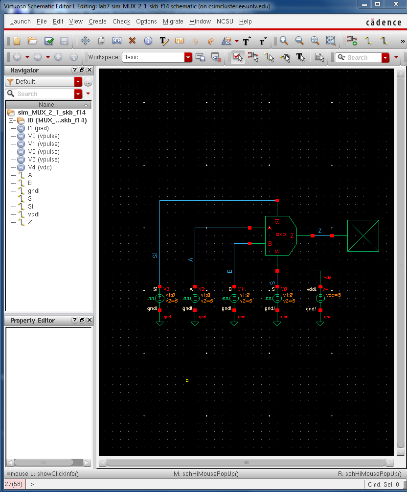
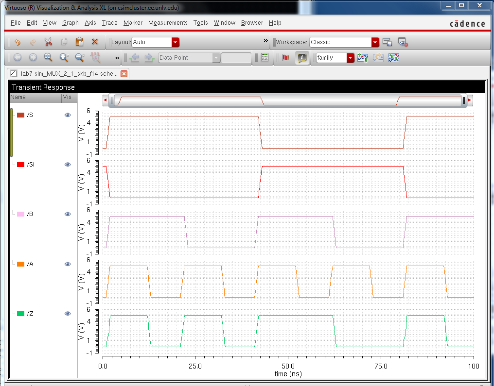
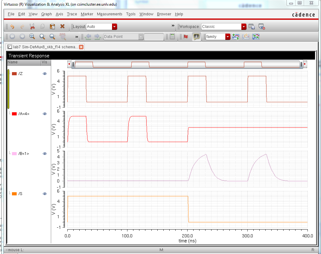
In the simulation above we can clearly see the Mux both MUXing and DEmuxing it's inputs, the operation is determined by what select we feed into it. It is worth noting that S and Si are merely inverses of each other and can be taken out of the design simply by inverting one input. Now that we have verified the first design we will verify the inverter idea.
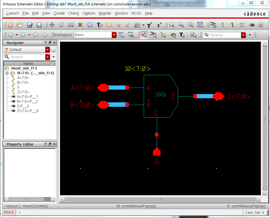
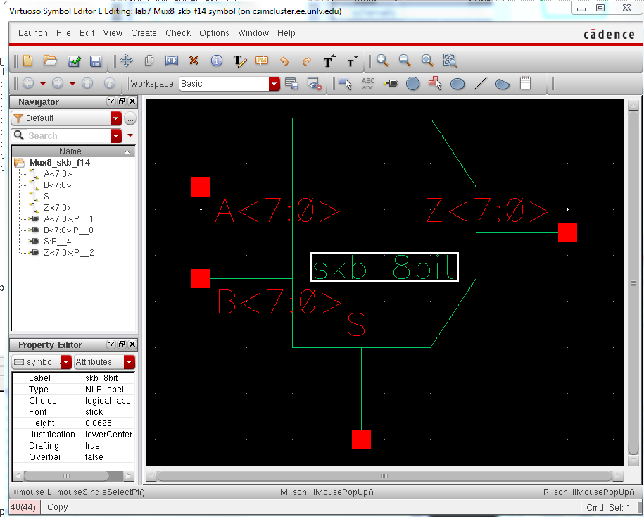
Since the lab requires an 8 bit version of this we will save the simulation for the 8 bit version shown below.
Under our new simulation we can clearly see that our design works just the same (no additional lag since this is not a cascade design). Next we will create our 1 bit adder and then our 8 bit adder. Last week we created an adder out of NAND and NOR while this weeks will be out of very simple PMOS/NMOS basic components. By creating the adder out of PMOS/NMOS on the most basic level we are able to cut down on the number of actual devices since it is a minimized design. This means that our new adder will act quicker than last lab's and also cost less to produce.
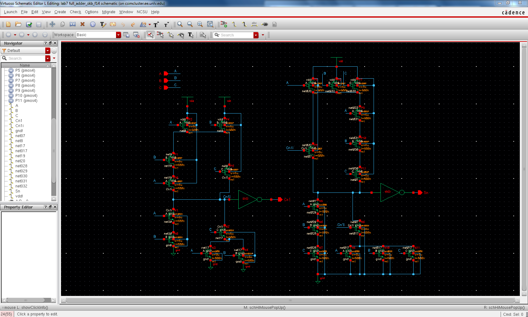
To build an 8 bit version we will first need a 1 bit version to cascade and use as a building block. I used metal2 for most horizontal connections while using poly and metal1 for the vertical connections. This allowed me to minimize my design while still keeping it clean enough to follow.
Now that we have the 1 bit the heavy lifting is out of the way. All we need now is to create 8 instances and add the pins while cascading the Cout to the C input of the next.
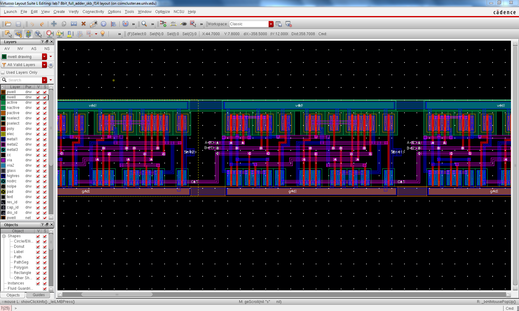
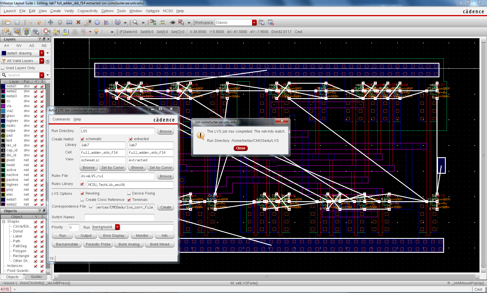
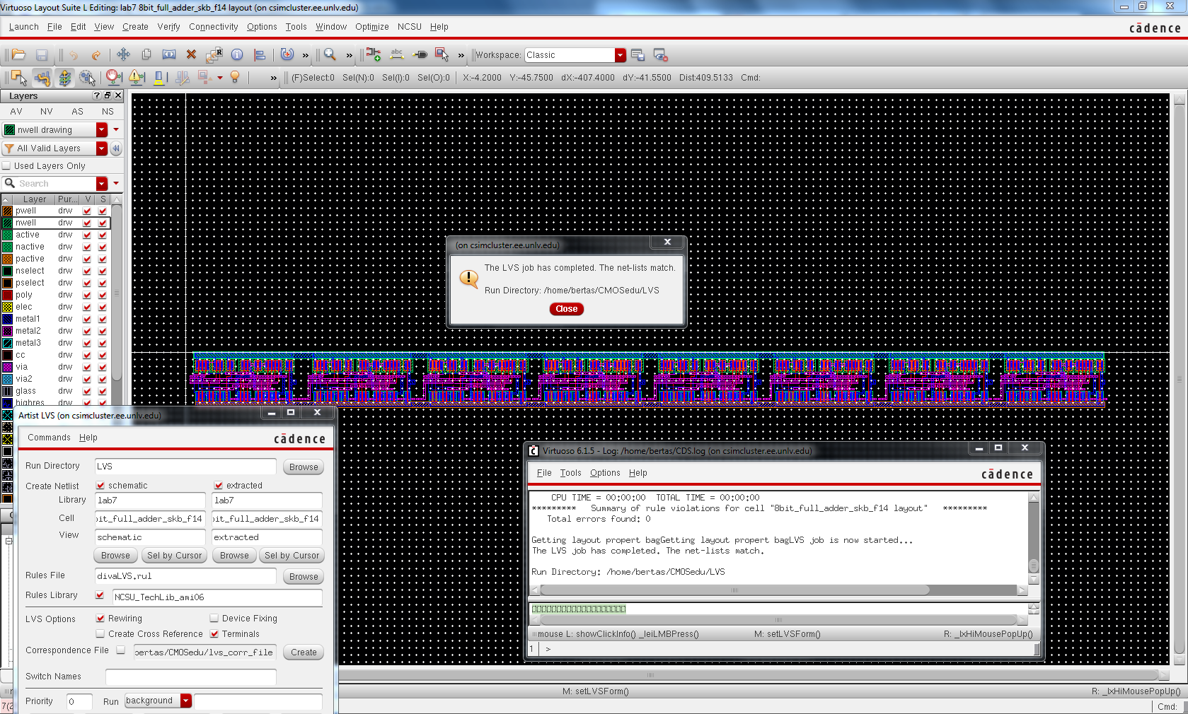
This will give us an overall layout which must be DRC'd and LVS'd against an 8bit schematic as seen below.
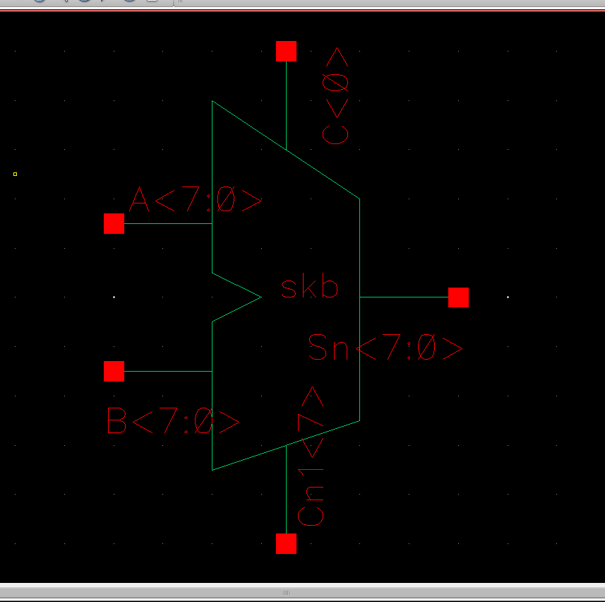
Now that we have a verified layout we can begin to create our symbol that will be tested.
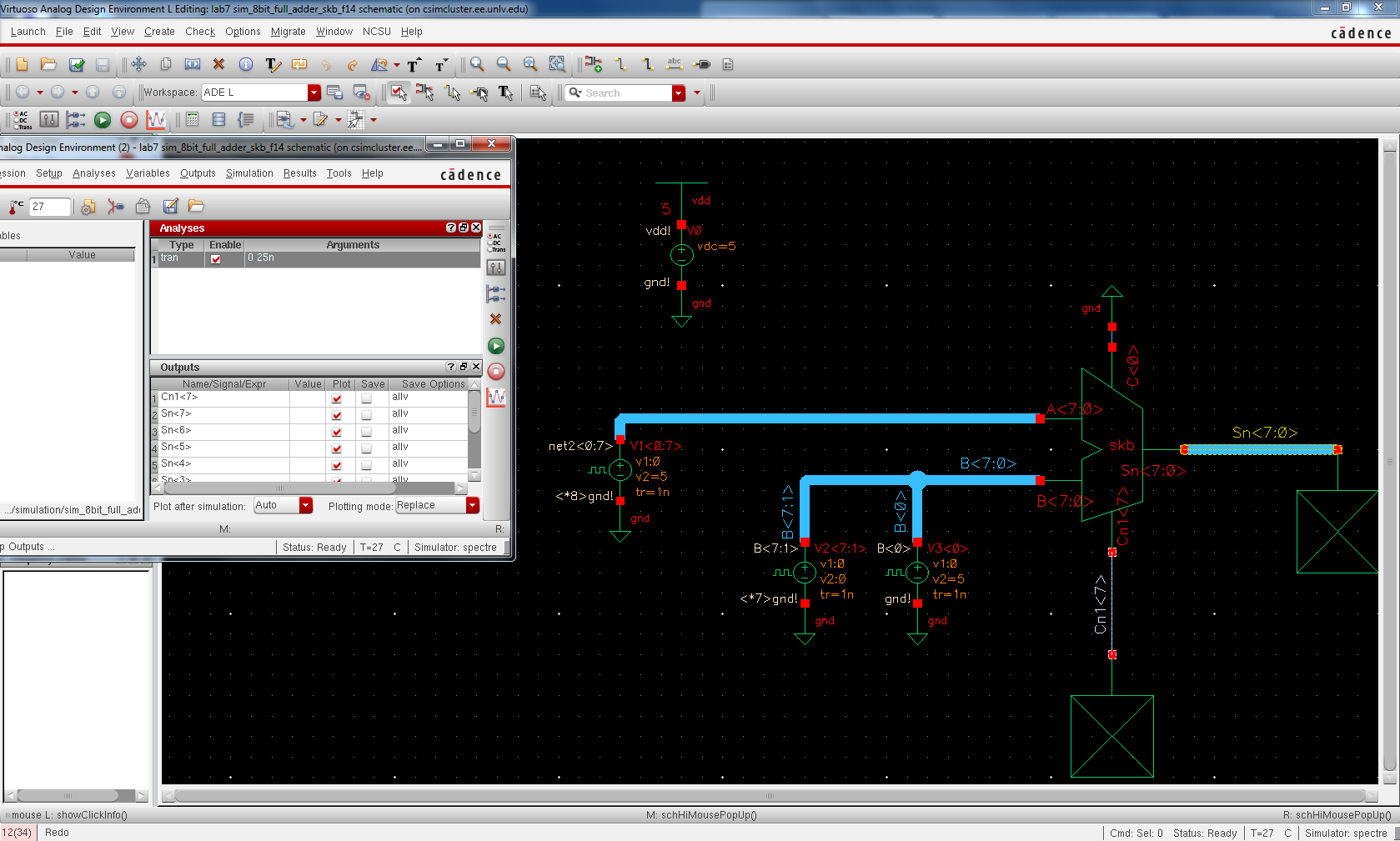
To test our design we must use various inputs and independently verify the outputs. This would be tedious and take up too much room on this lab to show all outputs and as such I have prepared a basic test that shows it performs as required. Any further tests can be verified by downloading the files and running various simulations. In this example we feed in 00000001 and 1111111 to produce 00000000 and a carry out of 1. This isshown by our outputs.
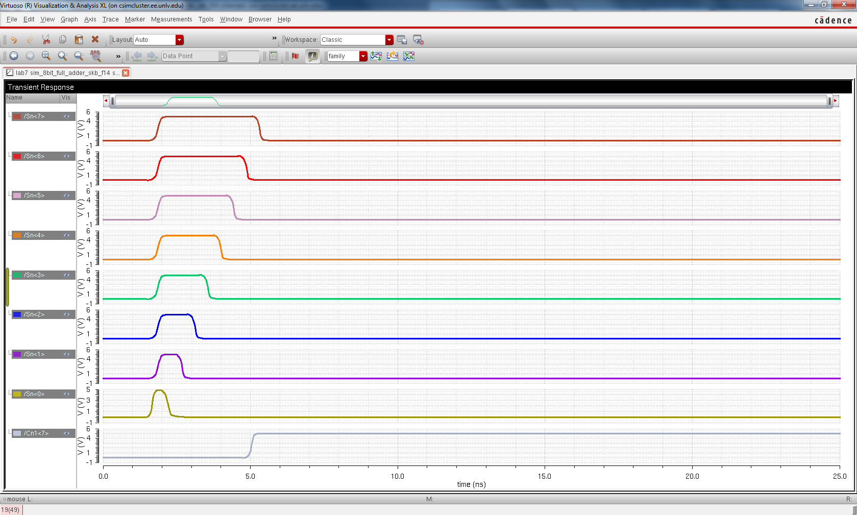
One important thing to note in our simulation is that since the each carryout is cascaded into the next bit there will be a delay associated with all the outputs. This is seen clearly above as the difference between the first bit Sn<0> and the last bit is close to 3nS. In design this time could be so small that we shouldn't worry or if you are working on a very large scale it could throw your whole design off.
After finishing the lab the files were backed up.
The files for this lab may be downloaded here.