Lab 06 - ECE 421L
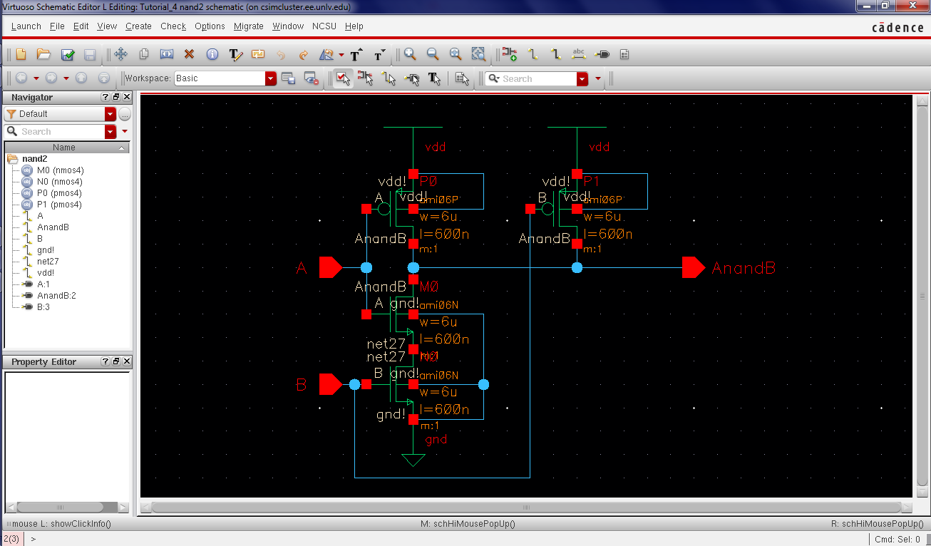
Lab 6: For this lab we will be creating a Full Adder out of NMOS and PMOS. We will start off by first creating the neccessary components that make up a FA (full adder): the NAND gate and the XOR gate. Below I started with a NAND.
After designing the schematic we will begin to layout our NAND to later be used in our FA.
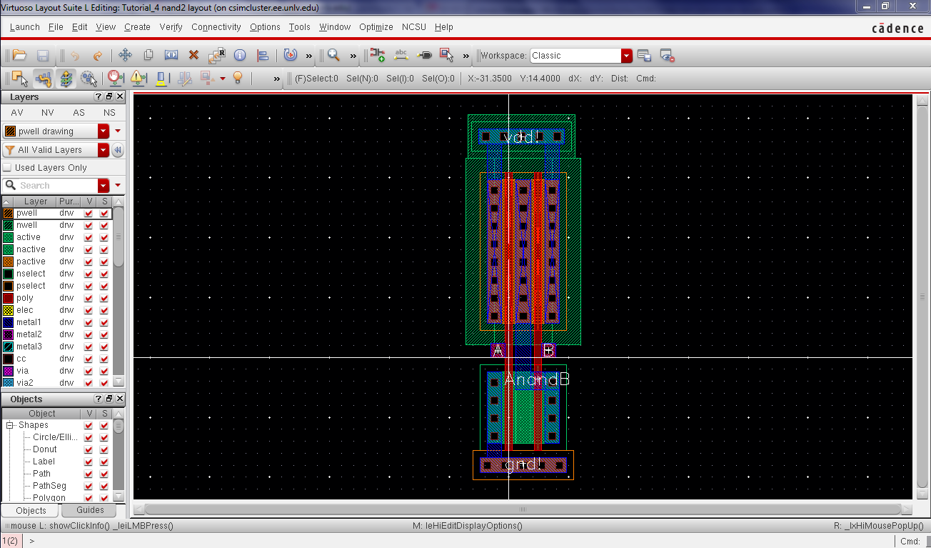
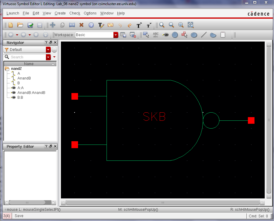
The layout for a NAND is quite simple being that it is just 2 PMOS and 2 NMOS. After making the appropriate conditions we will create a symbol allowing us to later test all of our gates.
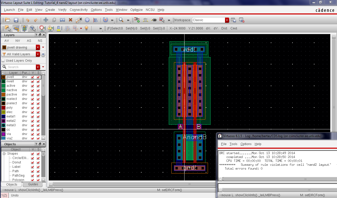
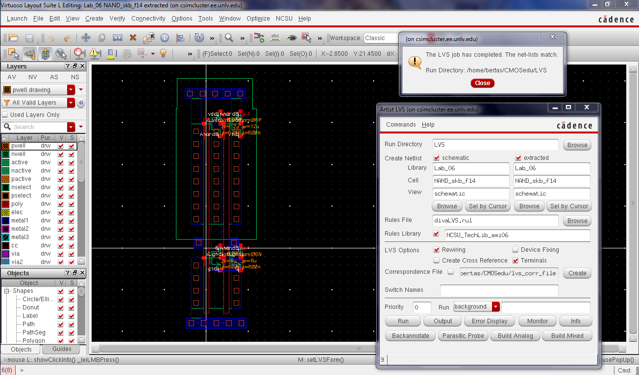
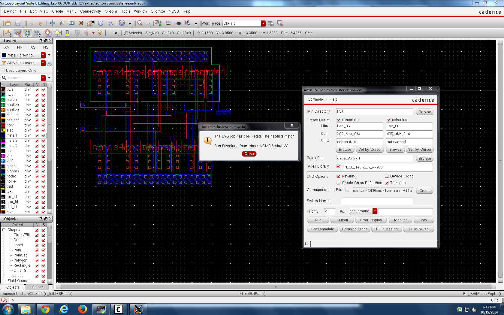
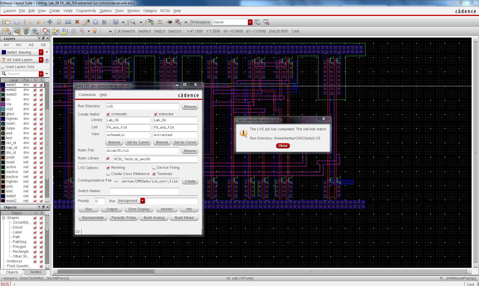
After running a quick DRC and completing the symbol view we will then LVS our layout to the schematic to ensure that it was made correctly.
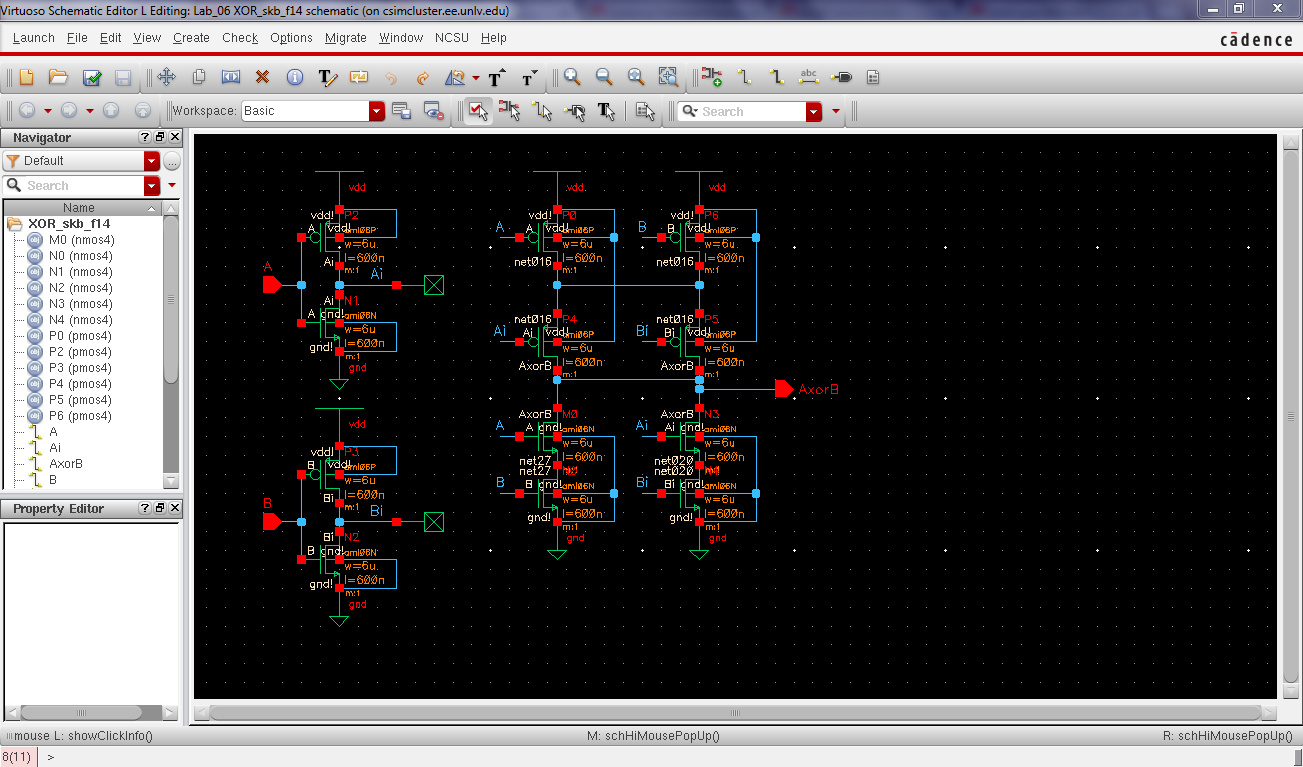
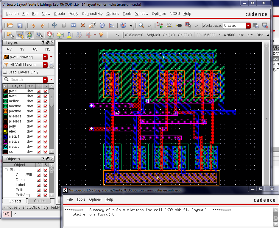
Now that our NAND is done we will move onto the XOR which has a much larger layout and will require more PMOS and NMOS. The schematic is done below and we will use this as our baseline to then create our layout.
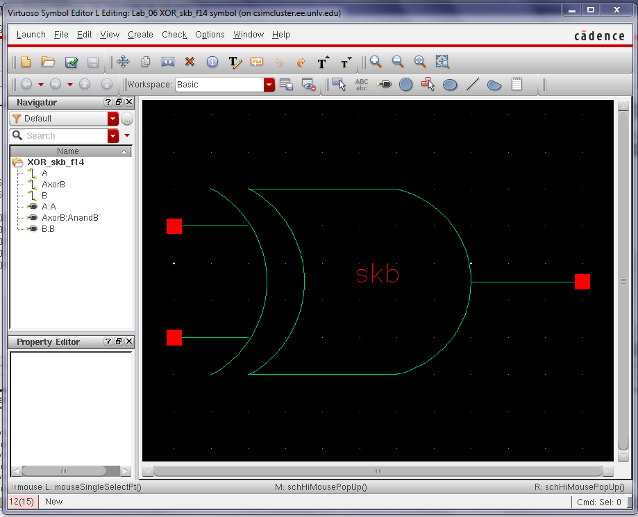
Below is the created symbol view that will be used to test our blocks both in the schematic of the FA and in a seperate test simulation of all our gates.
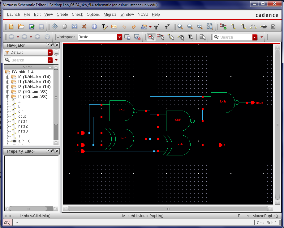
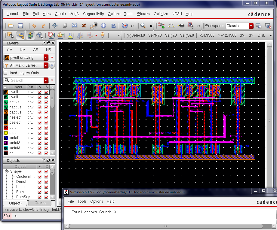
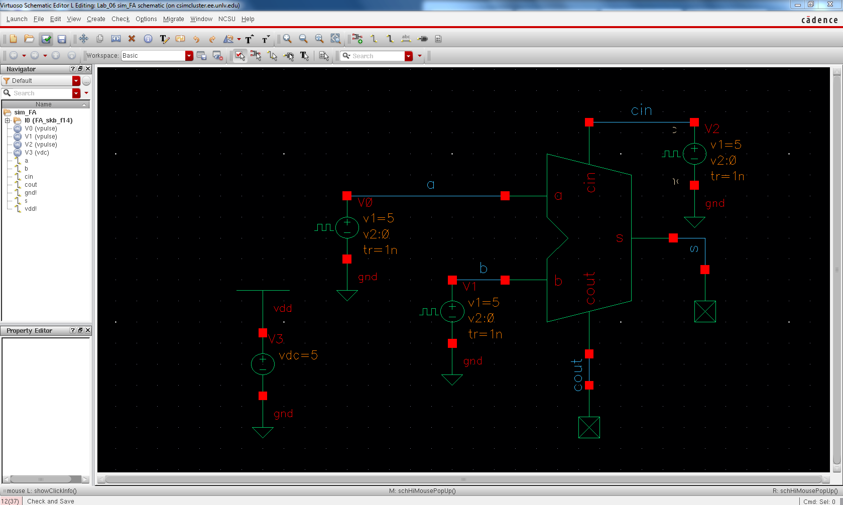
After we finish DRC and LVS we are ready to begin laying out our FA. We will start as usual with the schematic as seen below. When we move onto the layout we will insert the blocks we created for our NAND and XOR gates, to edit them into one cohesive unit we will "flatten" the layout as seen in our Tutorial 4 in lab. By flattening we can edit the entire schematic together and allows us to make the connections clearly.
After the DRC and LVS we need to test our schematic to ensure that it runs as designed. We will create a symbol for this and simulate it as needed.
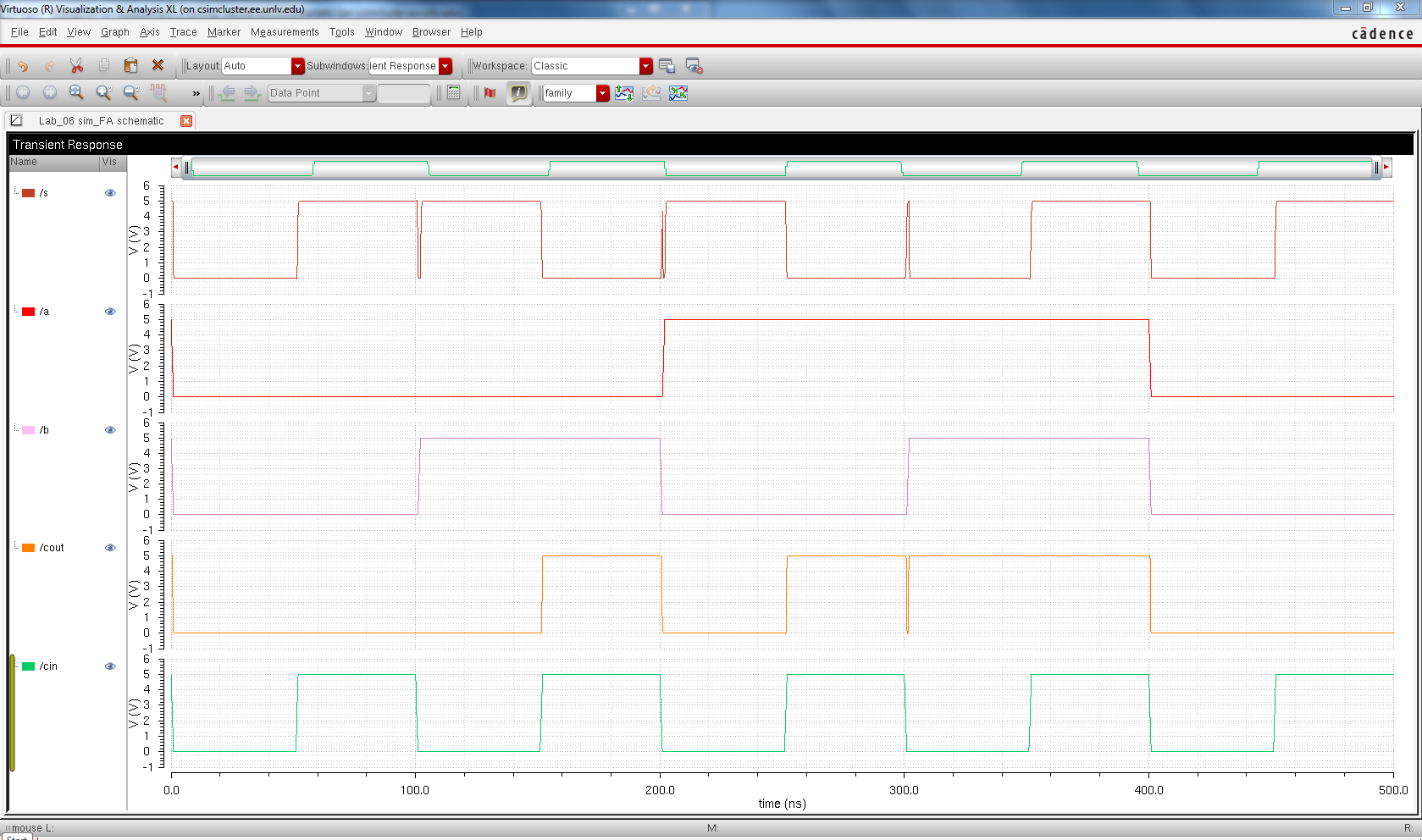
Below
we can see that our schematic runs as required. We feed an input of 00
in and our output is 0, at 10 or 01 the output is 1 and if we feed in a
11 we will see that we get 1 and a cout (carry out). So our schematic
runs as expected however, we can see that we occassionally get some
blips on our graph; these are caused by the rise/fall time associated
with our logic. This is unavoidable at the nano scale that we are using
and is just a factor of our logic delays.
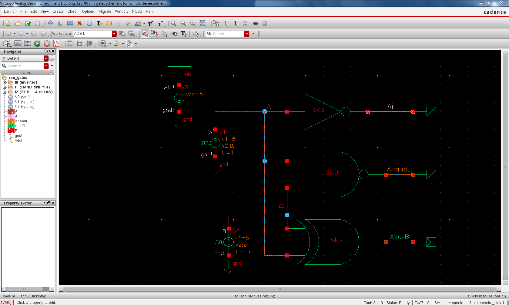
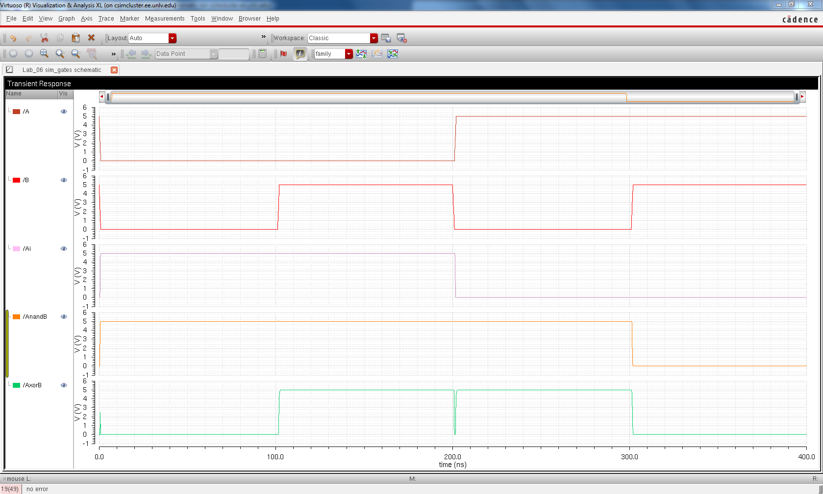
We will also simulate all our gates to show that they individually work. These are the three fundamental gates that we have made to date in our lab class. The DRC, LVS and layout of the inverter are not covered here since we built those last lab and we did not make any changes to them in this lab. Once we put all these gates into the schematic we simulate it and see that all the outputs work as expected and once again the small blips are due to the rise/fall time associated with the input.
Files were then backed up.
The files can also be located here.