Lab 05 - ECE 421L
In lab 05 we will be designing a CMOS inverter and testing/verifying all aspects of this design (simulation, layout, etc.).
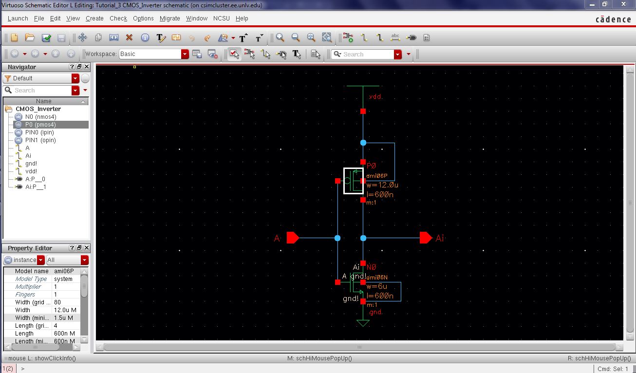
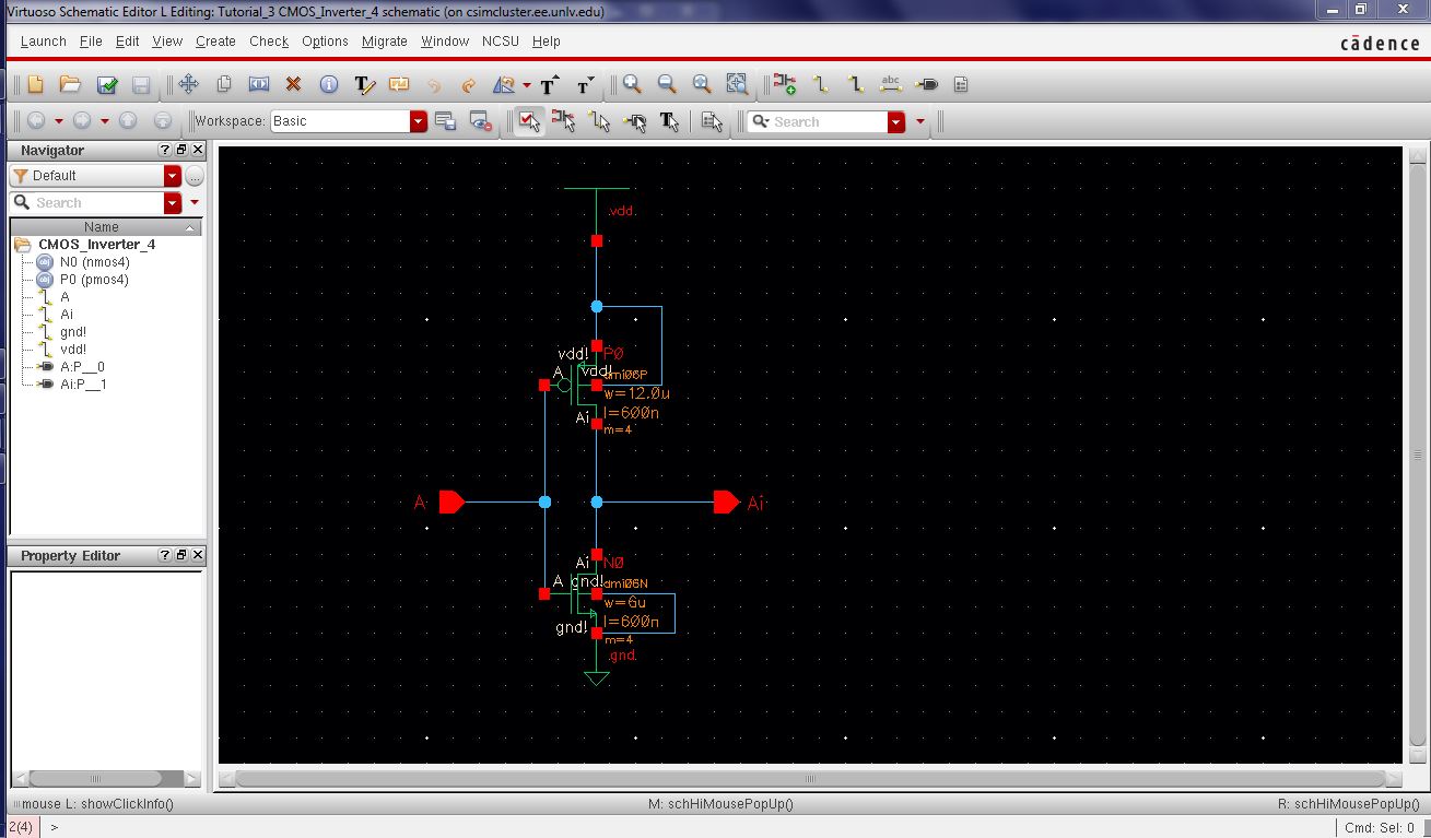
First we start off by laying out a schematic that we will use to run our LVS down the road. We will be creating two of everything one for a typical inverter and another that has a multiple of 4 for both the NMOS and PMOS components.
After creating the schematics we will move onto the actual layouts.
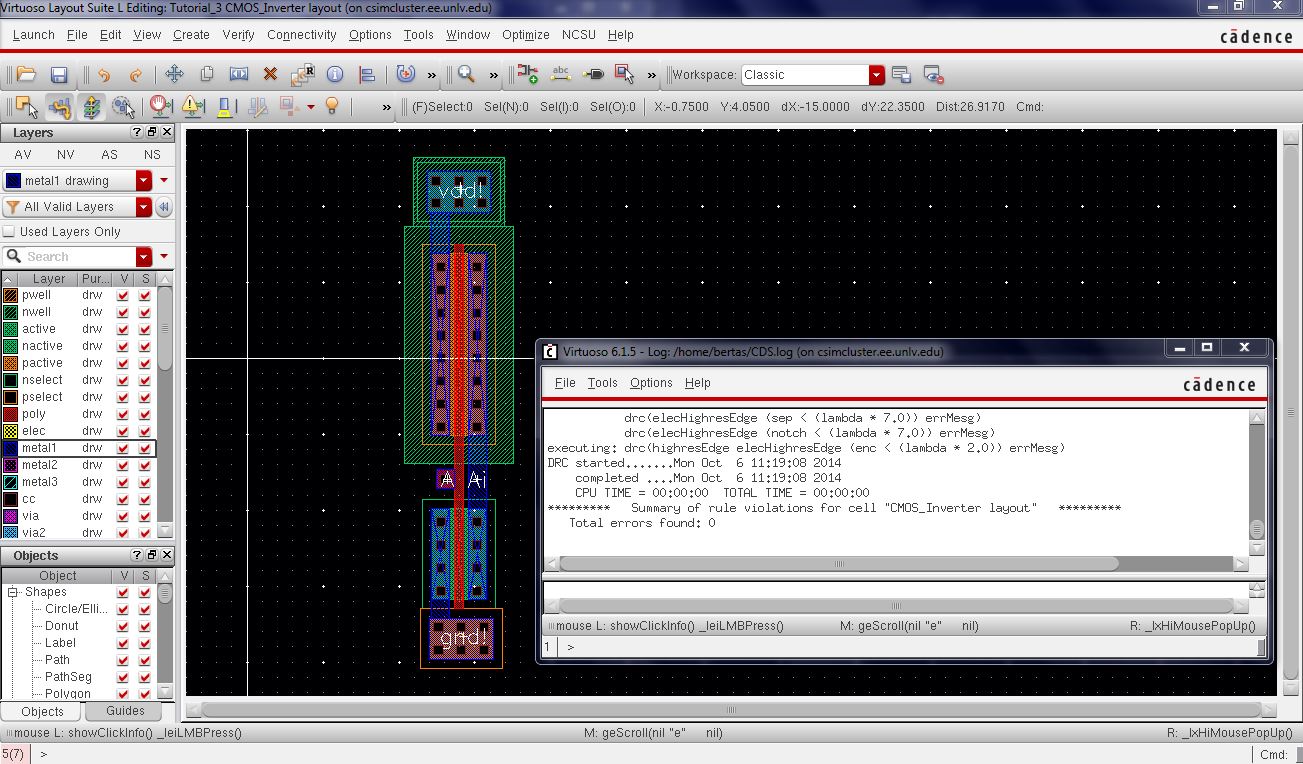
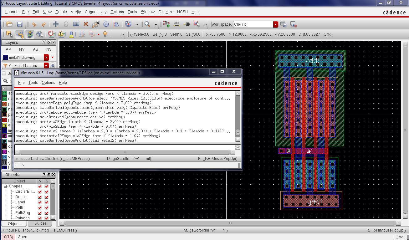
After creating these layouts we will DRC both and then also LVS them with respect to their schematics after extracting them. It is important to note that the two layouts are almost identical except that the second layout is composed of 4 NMOS and 4 PMOS.
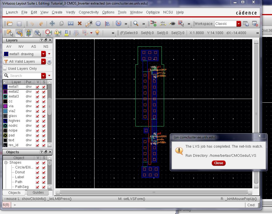
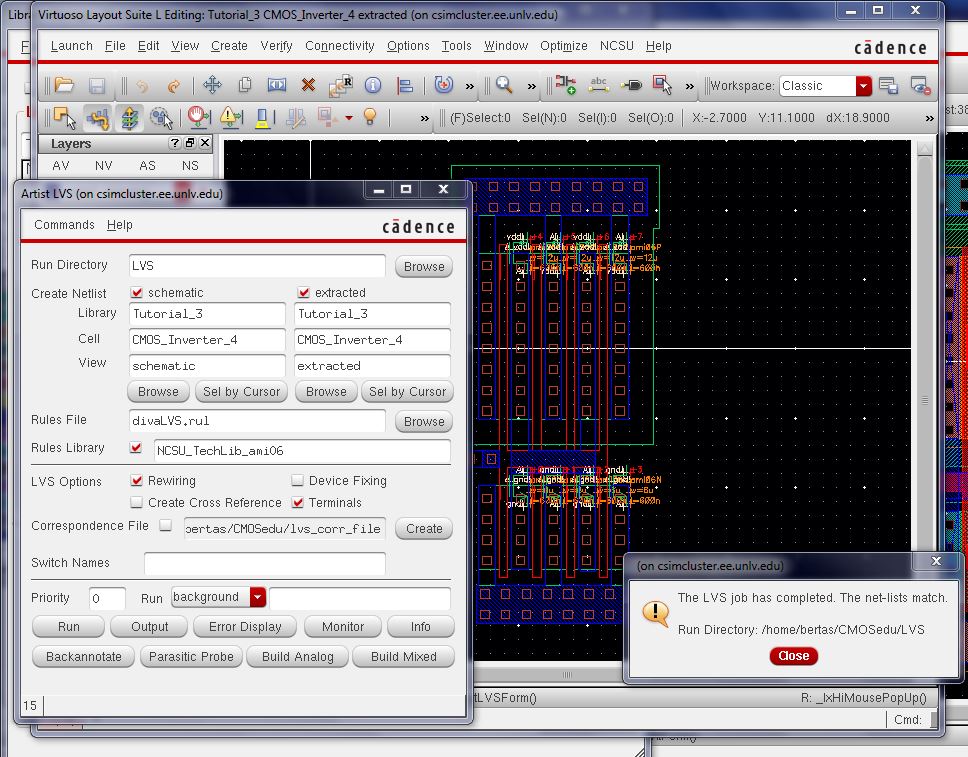
After the LVS has completed with no errors we proceed with creating a symbol for both of the layouts.
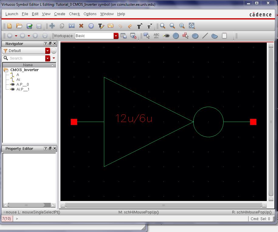
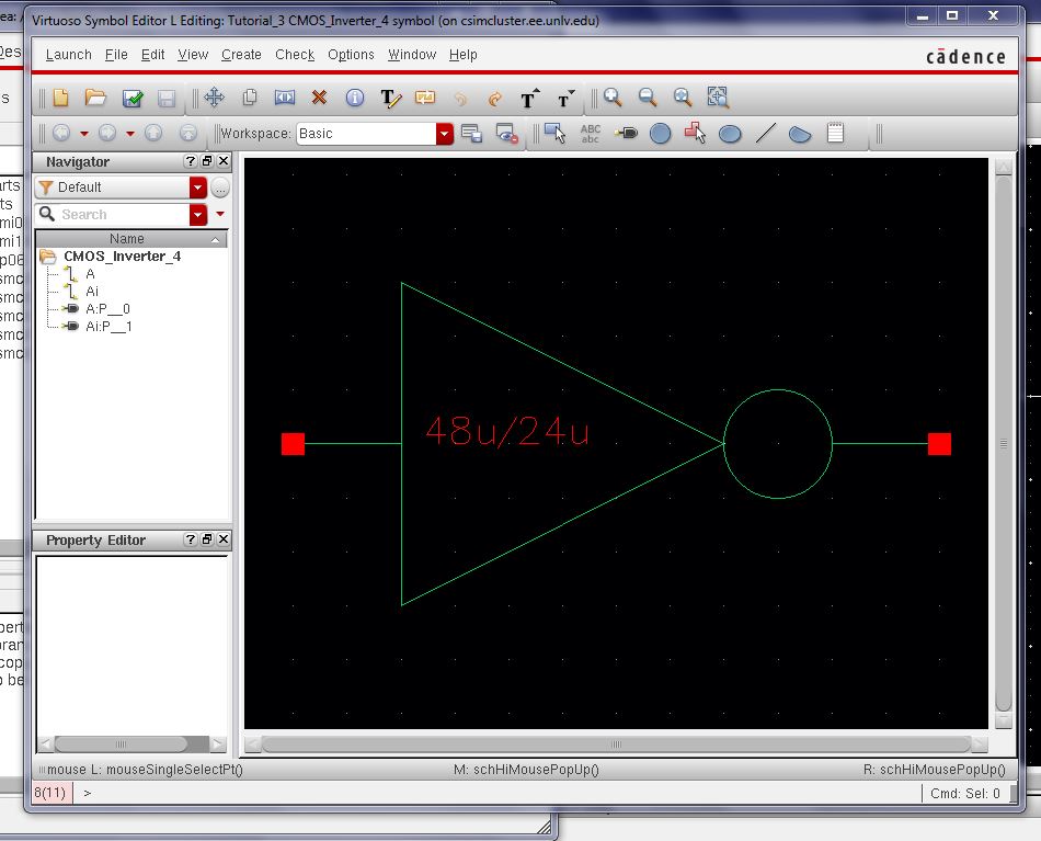
The symbols are named with the respective dimensions that associate with them. By naming these symbols we will be able to easily identify them in our simulation schematics. Next we will begin simulating these symbols and verifying that they react the way we want.
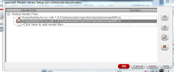
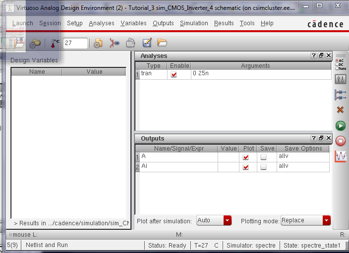
Before simulating however we must add in our models to our ADE L model libraries and also create our spectre state.
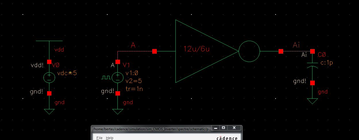
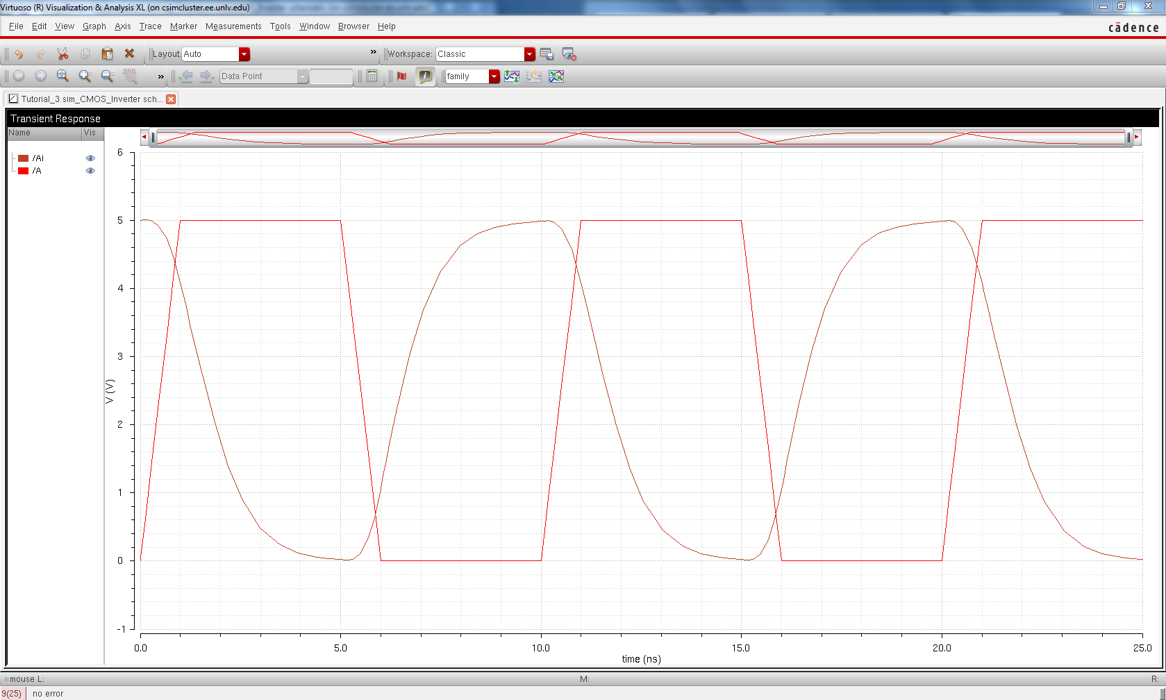
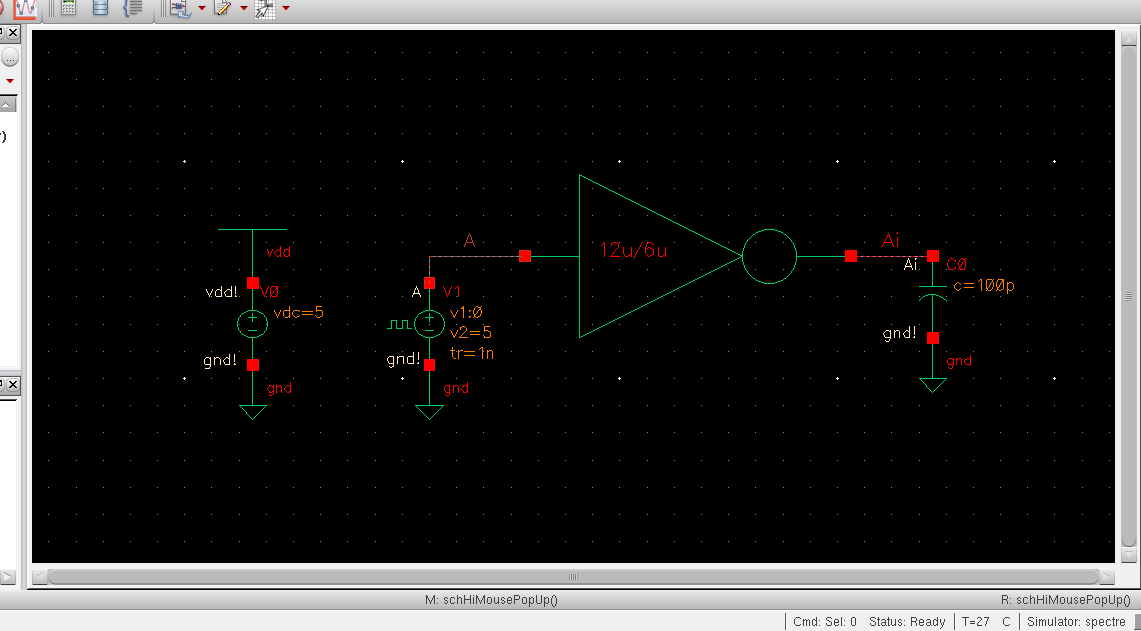
We will start off with the regular 12u/6u CMOS inverter.
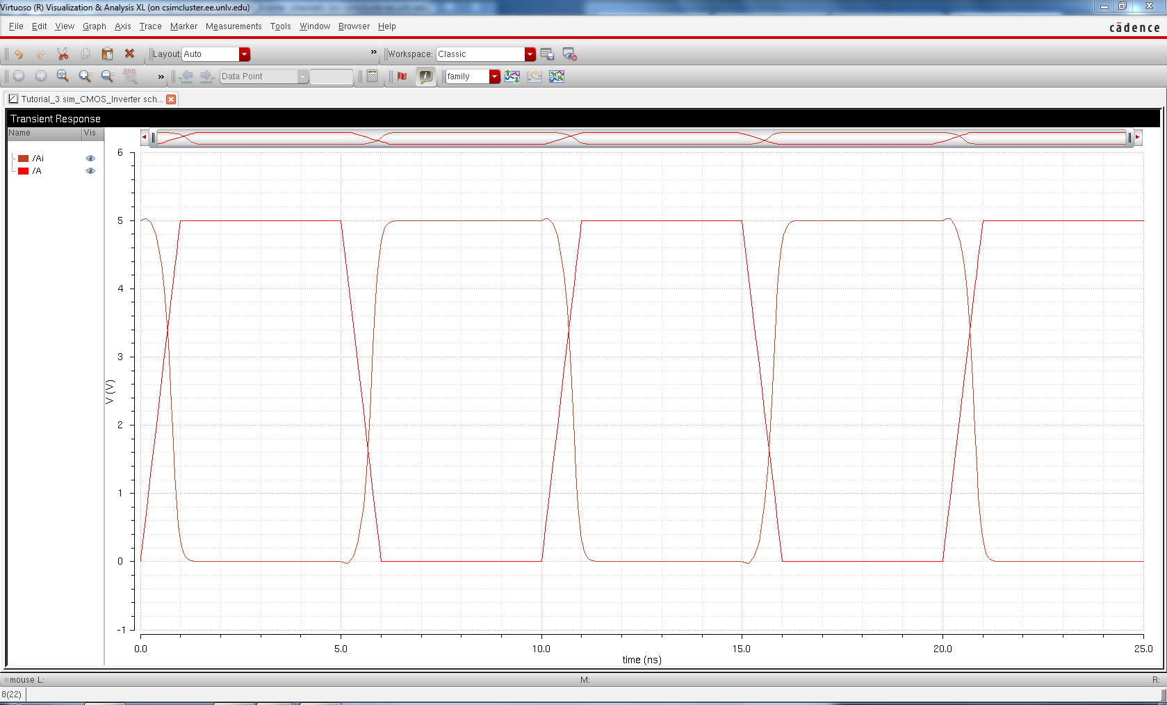
| Schematic | Simulation Results | ||
 |  | ||
 |  | ||
 |  | ||
 | 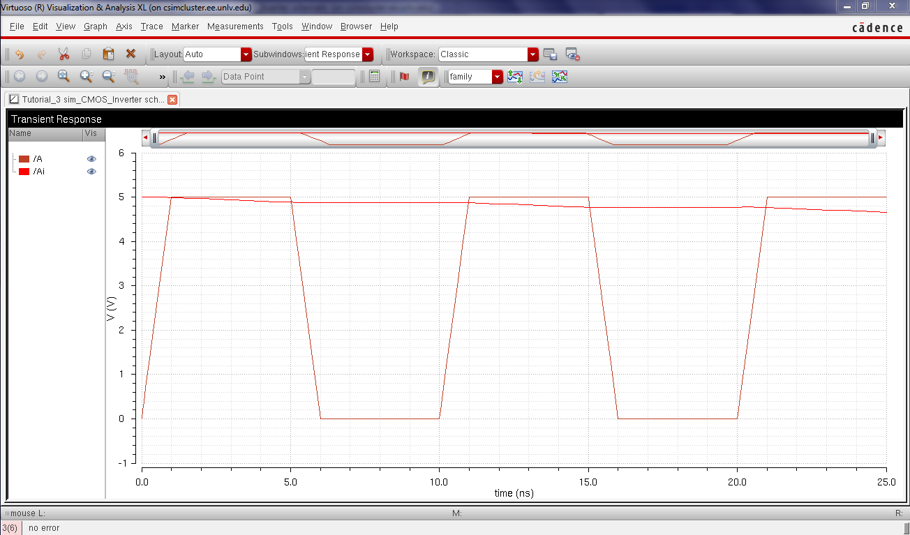 |
After simulating our first inverter we realize that our design operates as it was intended and inverts the signal however, the capacitive load creates a delay in the signal. This delay is causing our inverter to act much more slowly than it would without it and even makes it so that it will not fully invert the signal at the higher capacitances. This would be very important to note in any design to ensure that your inverter will fully invert your signal.
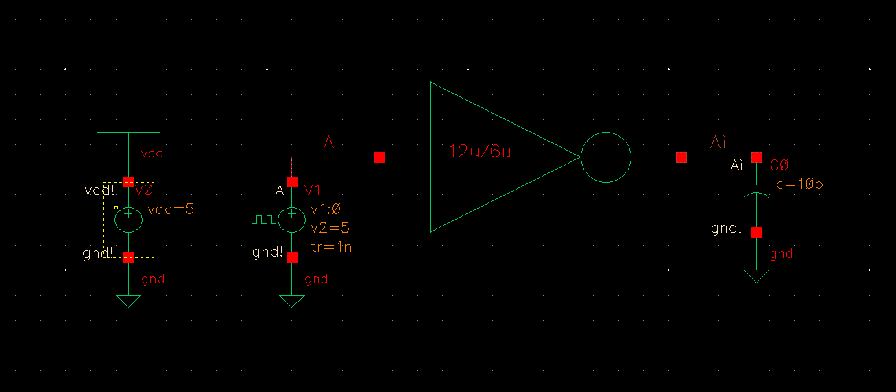
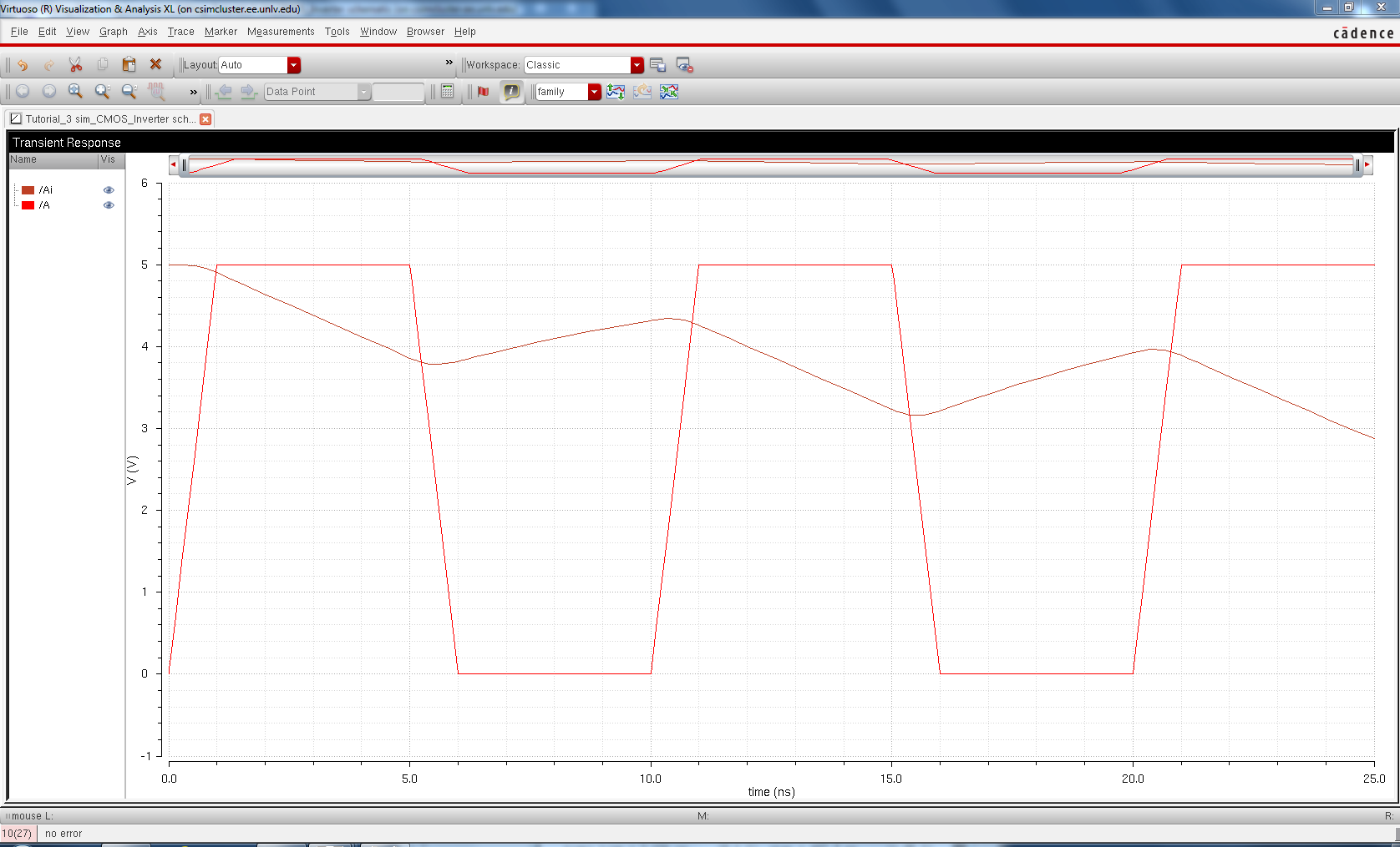
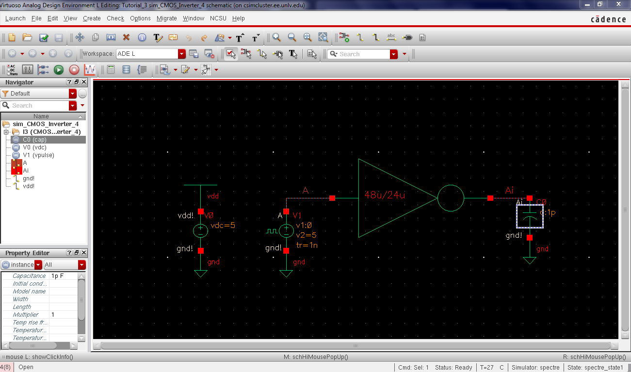
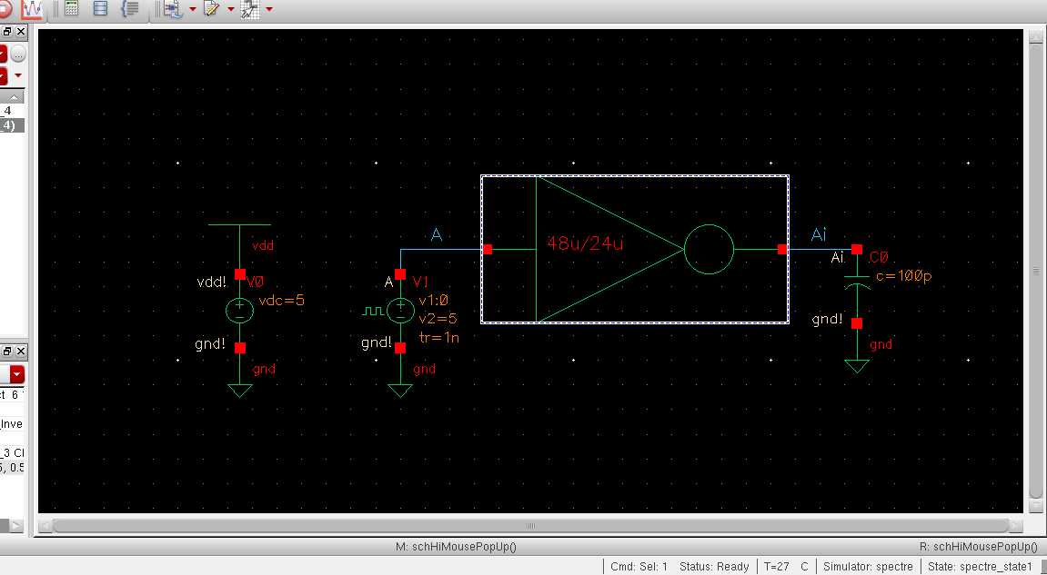
Next we will run the simulations for our 48u/24u inverter.
| Schematic | Simulation Results |
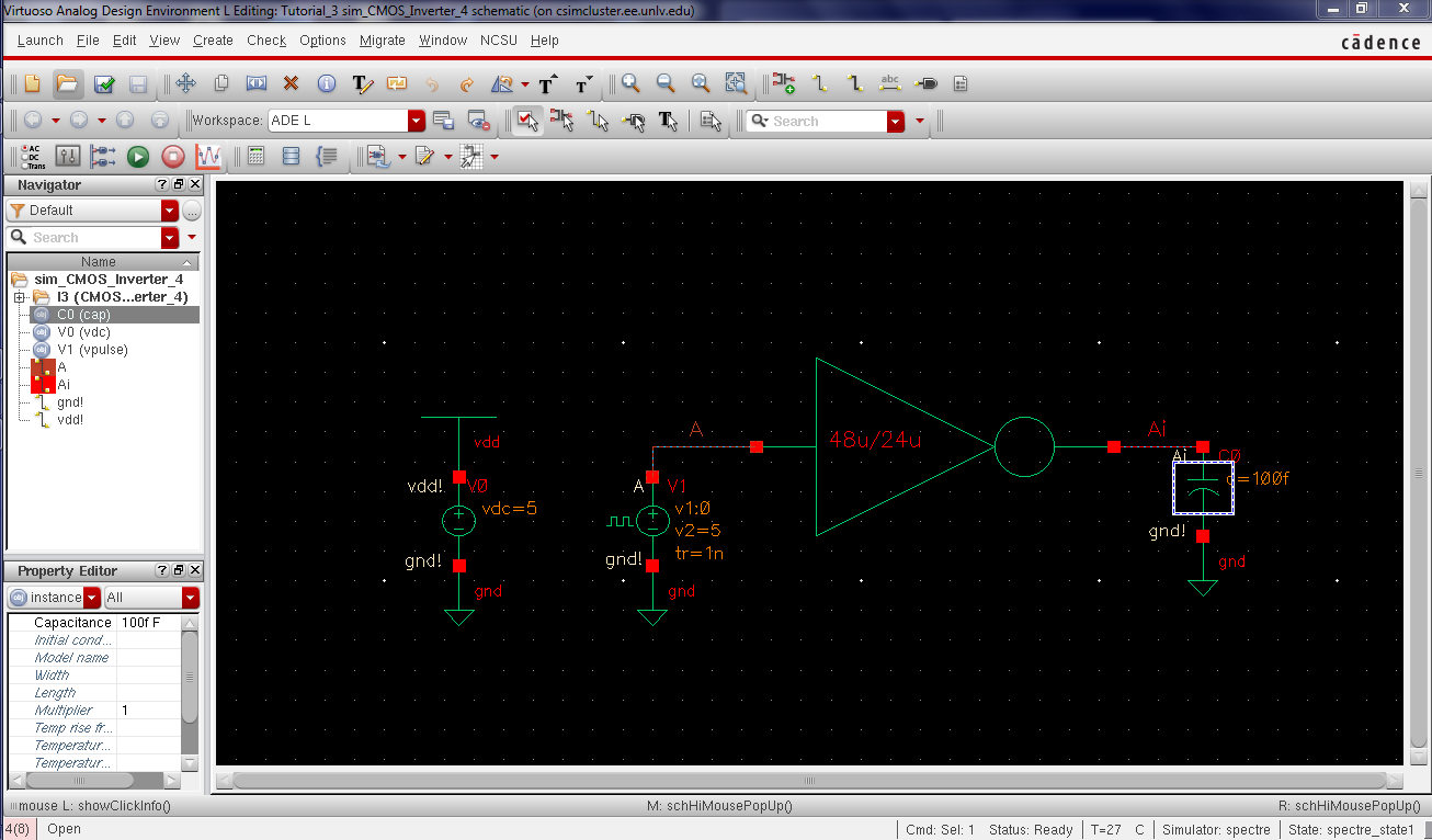 | 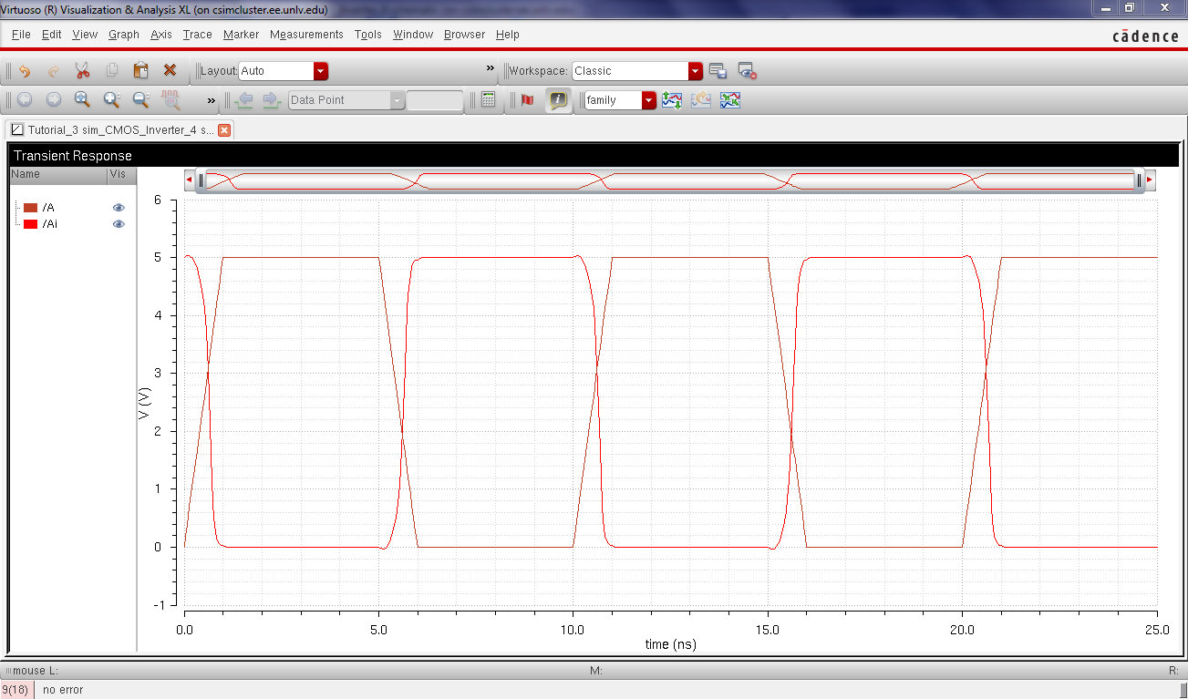 |
 | 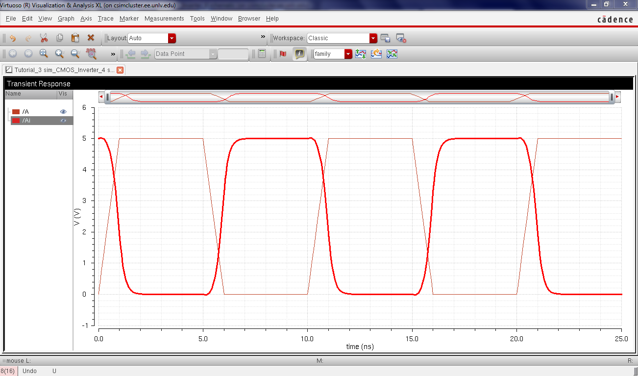 |
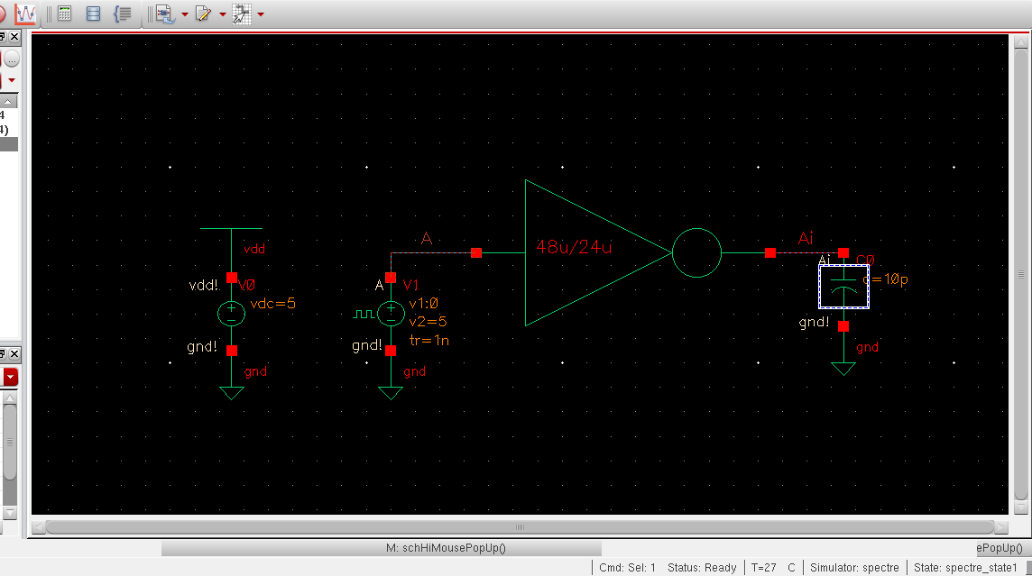 | 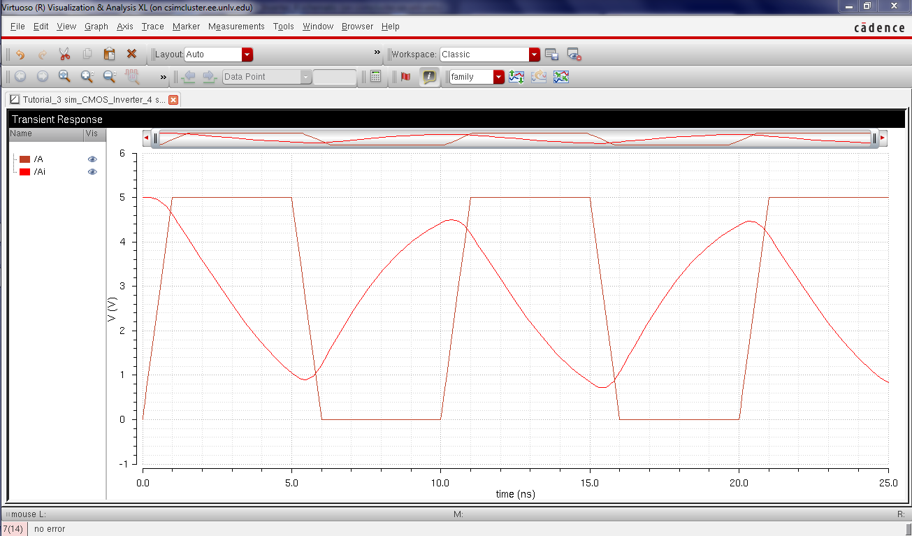 |
 | 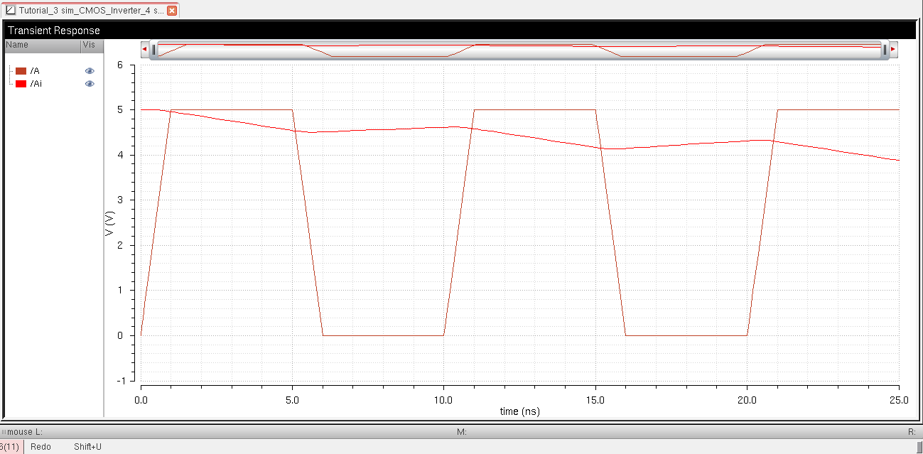 |
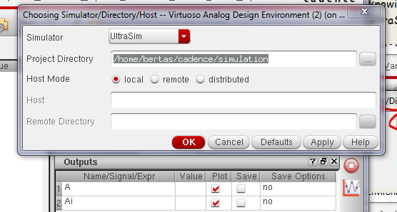
After analyzing both the inverters and their simulation results it becomes clear that the larger inverter switches much faster than the smaller 12u/6u inverter. By comparing the 100pico-Farad simulations we can see that the larger inverter can get to about 4.5V when the smaller can hardly reach around 4.9V. Next we will simulate the above schematics again using Ultrasim to see if there is a significant difference. Ultrasim is a faster simulation profile however, it is not as accurate as Spectre and can only run Transient analysis. Below we see the results, the schematics are not displayed since they are identical to those above.
| Capacitance | 12u/6u Results | 48u/24u Results |
| 100f | 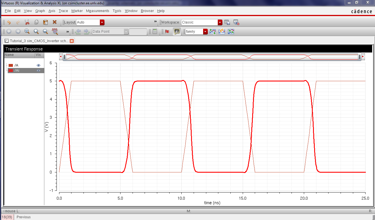 | 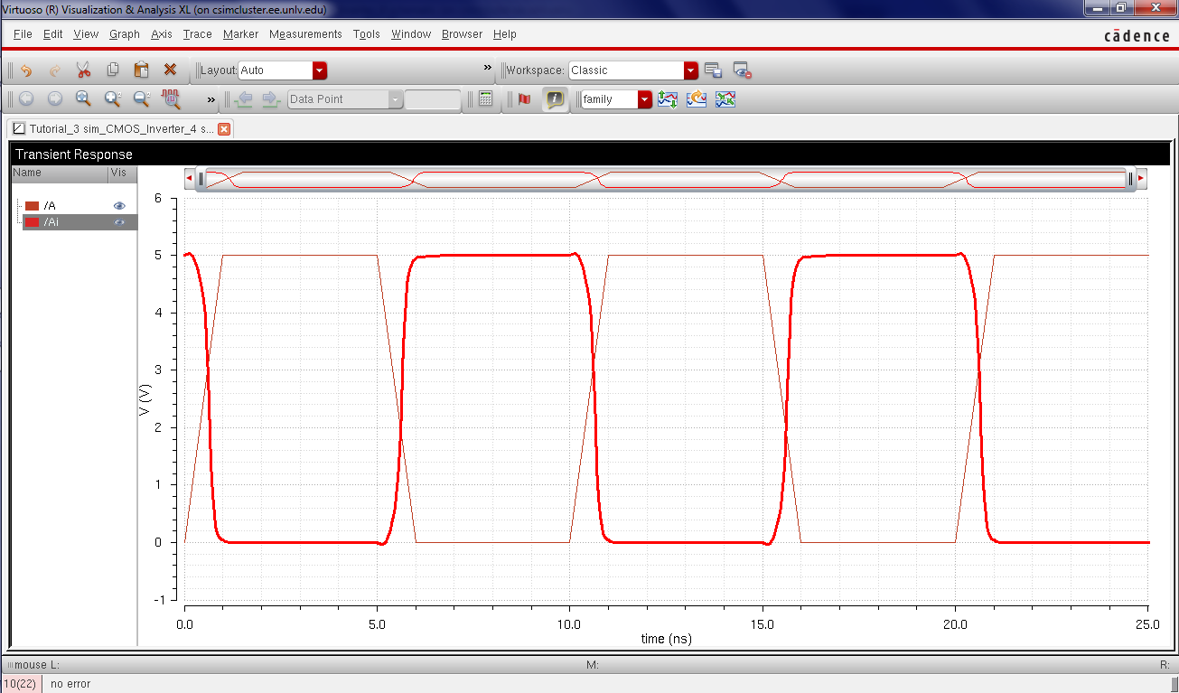 |
| 1p | 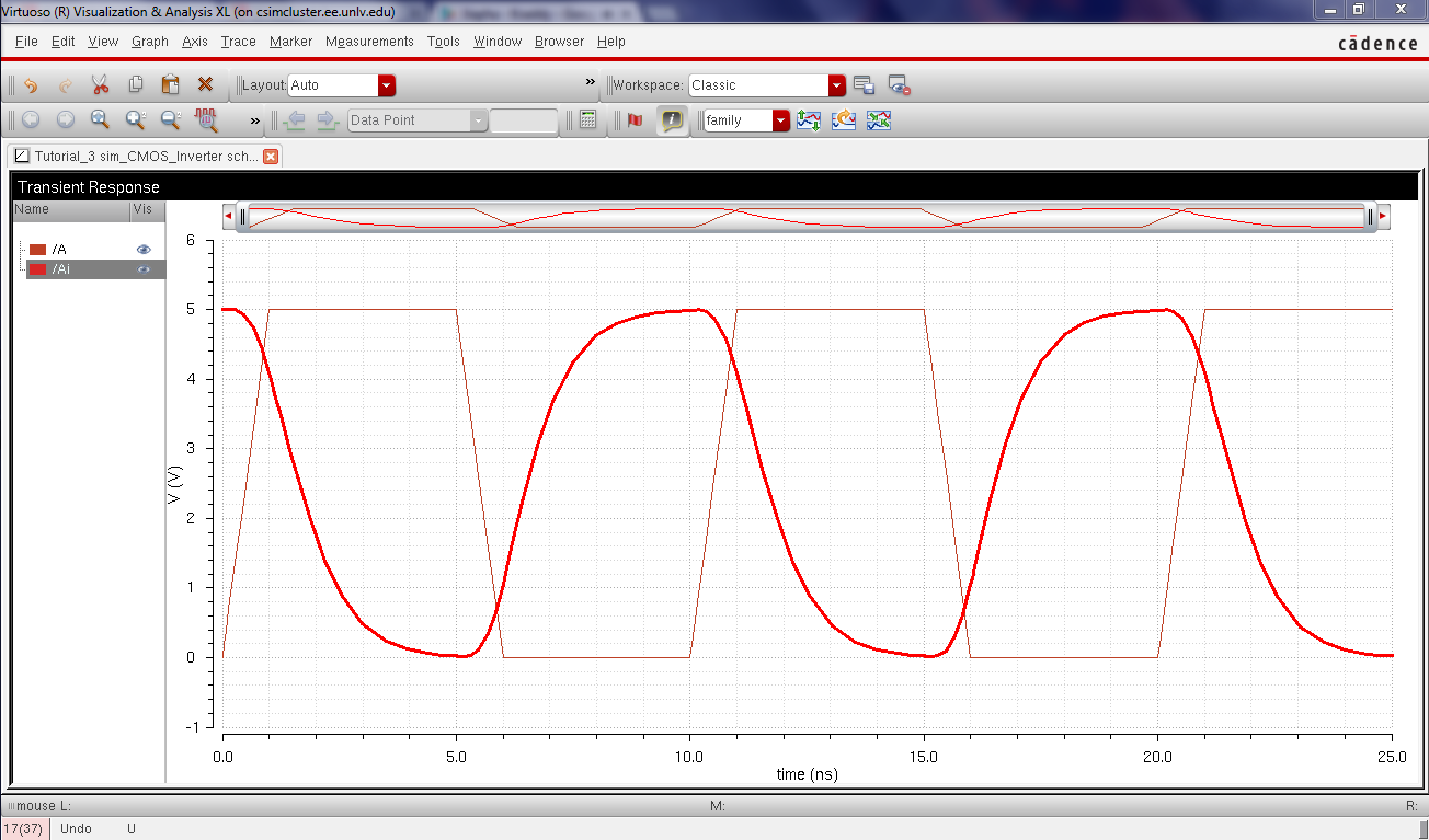 | 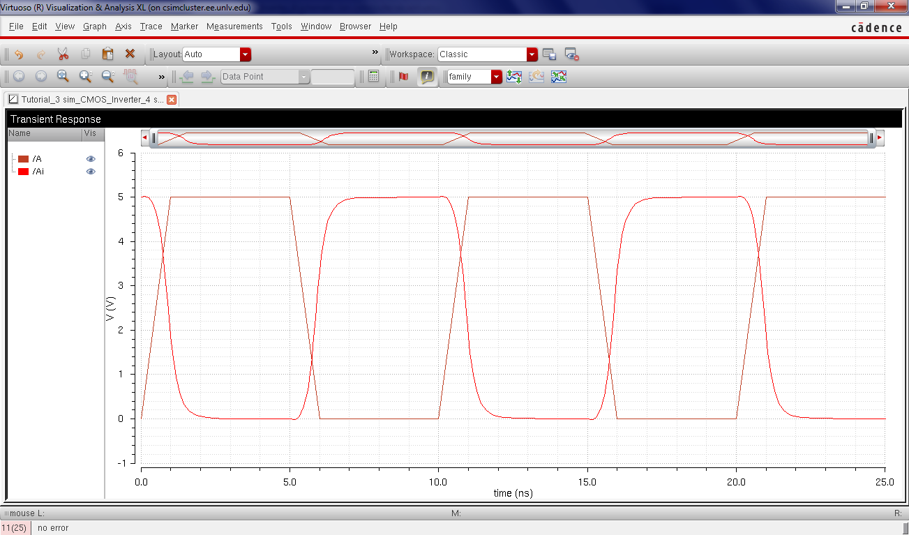 |
| 10p | 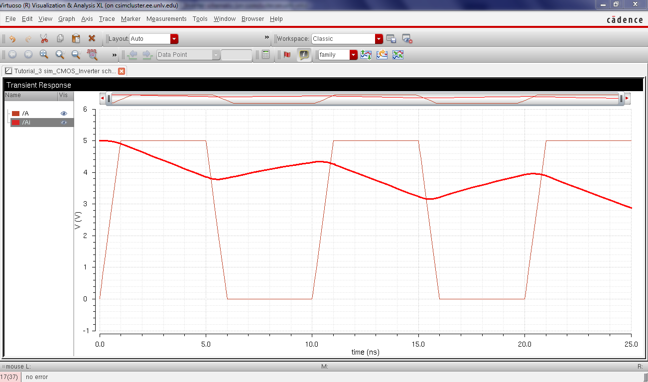 | 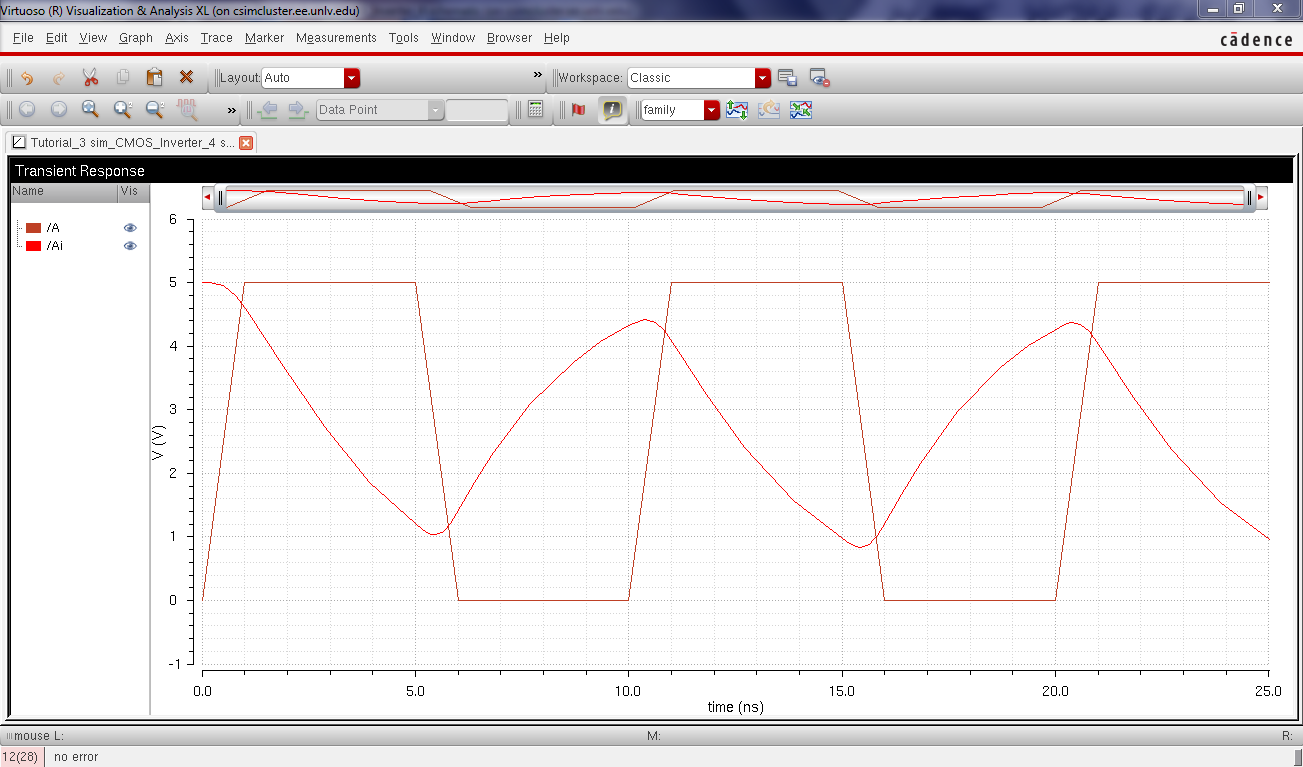 |
| 100p | 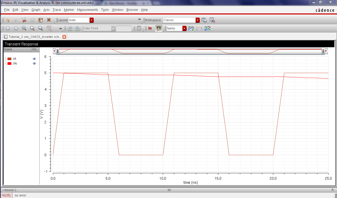 | 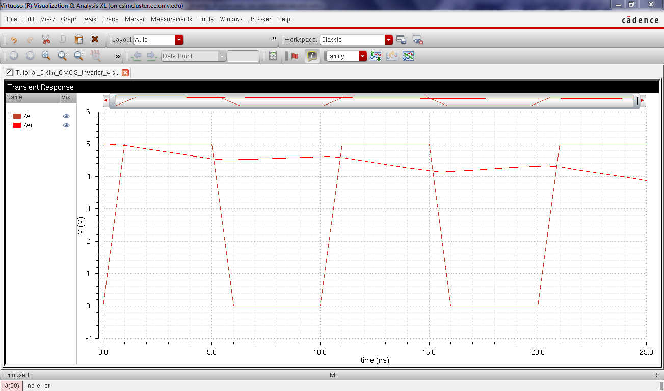 |
By comparing the ultrasim results with those above we can see a few instances where Ultrasim is either not as fast or just not as accurate (noticeable in the 100p case). Ultrasim is however close enough that it would be a good alternative if the schematics get much bigger.
Backed-up Files:
Files available for download here.