Lab 04 - ECE 421L
Lab 4: In this lab we will be generating IV plots for both PMOS and NMOS while also designing layouts for both.
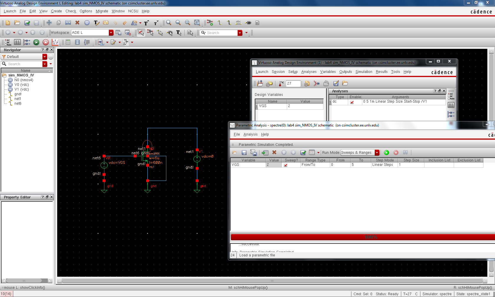
First, I opened Cadence in a Virtuoso window and created a new library for Lab 4. Next I began creating the cell views that I would need starting with the simulation cells for both NMOS and PMOS. After creating the schematic I opened ADE L to start the simulations and sweeps. The first graphs we will generate is ID vs VDS (VSD). In order to sweep variables we must go to the tools and then parametric analysis within the ADE L window (covered in several course examples and tutorials).
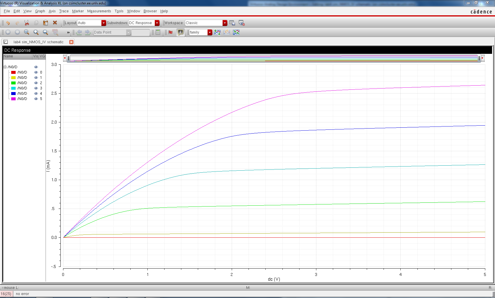
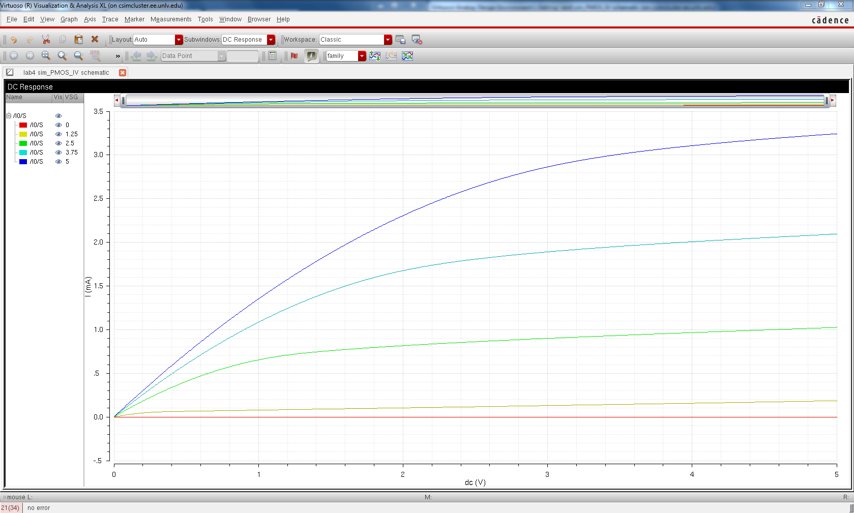
Below you can see the finished schematic that we will run as well as the settings used (however this must be run from within the Parametric Analysis window). The requirements were to VGS (VSG) from 0 to 5V in 1V steps as well as VDS (VSD) in the same increments.
Next
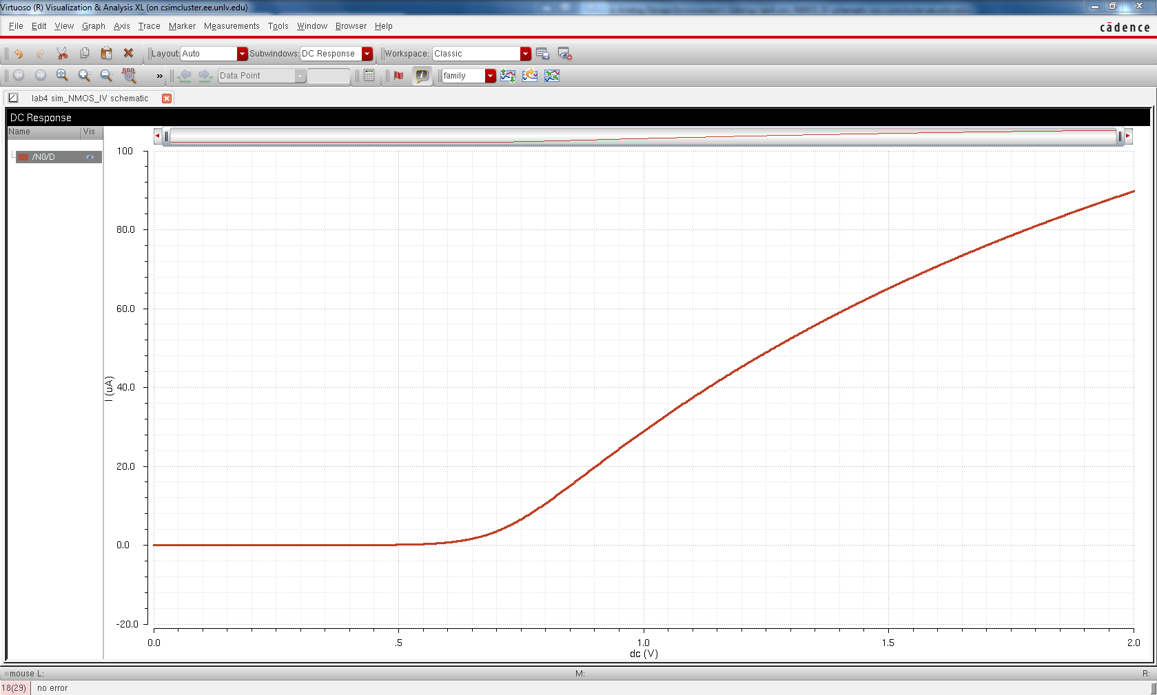
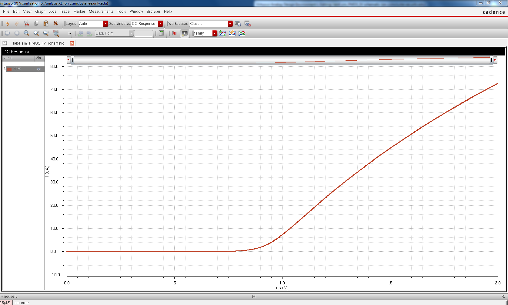
task we had was to create an ID vs VGS (VSG) graph. In this graph we
will be sweeping VGS and VSG from 0 to 2V in 1mV steps. NMOS: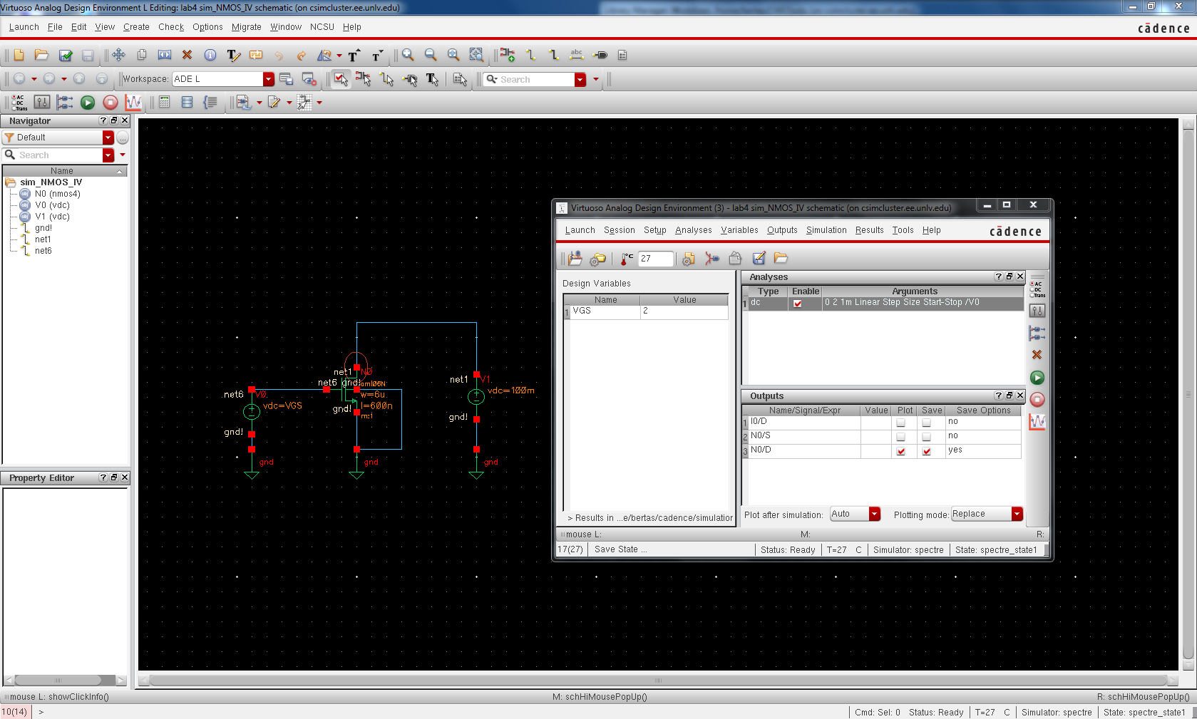
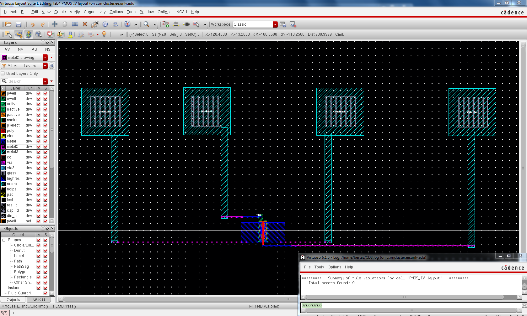
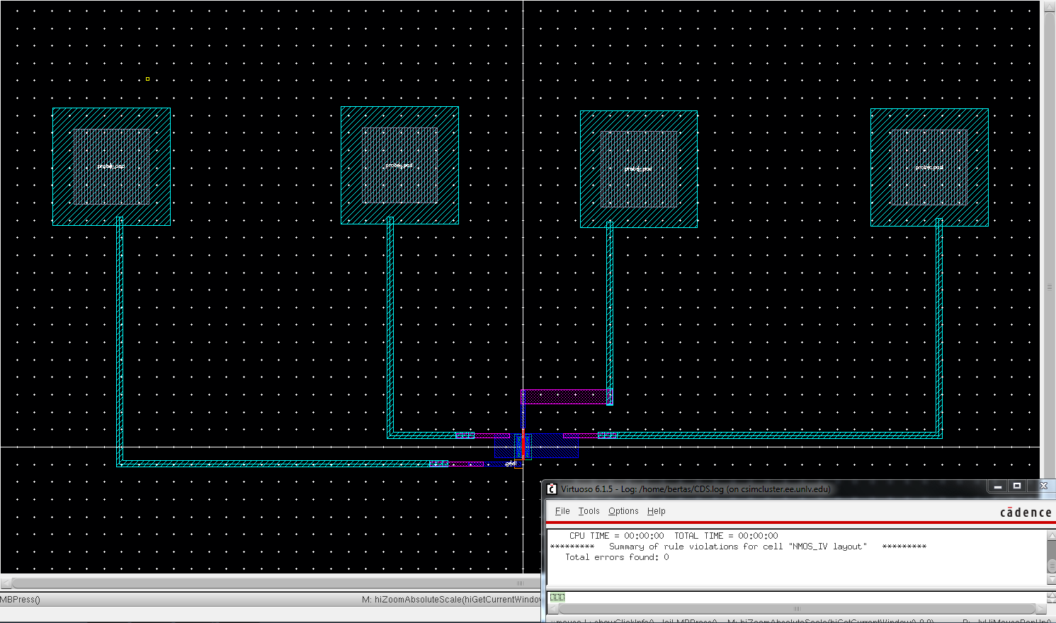
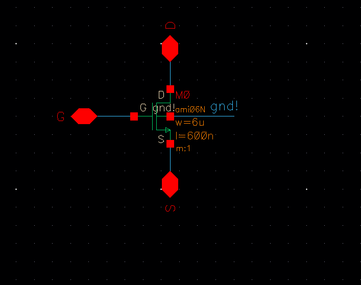
After finishing these schematics and simulations we had to create some layout views of the NMOS and PMOS, DRC them and then LVS them with reference to a 4 pin NMOS and PMOS (body tied to ground and vdd respectively). Below is the NMOS which can be very easily identified as one of the pins is labeled gnd! declaring it as a global and thus showing that the body is in fact tied to ground.
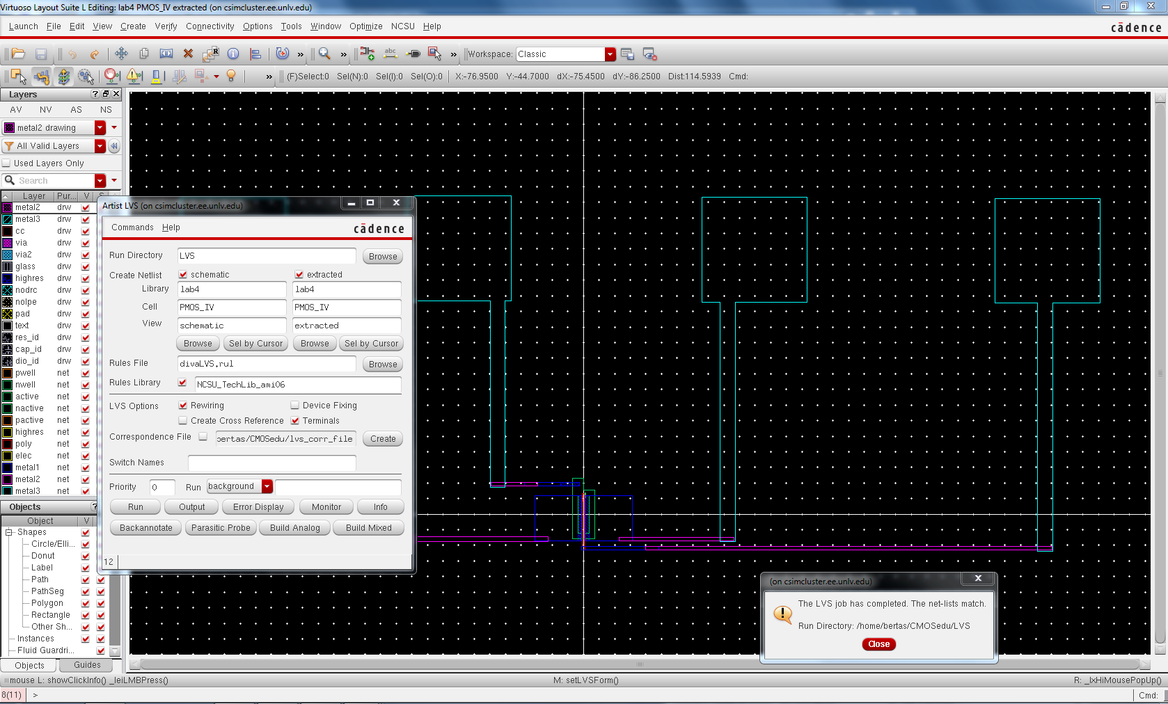
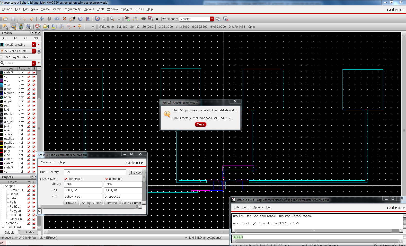
After running the DRC and preparing the schematic view we must now extract our layout and LVS it against the schematic to ensure the pins match. Below we can see the extracted view as well as the LVS completing successfully.
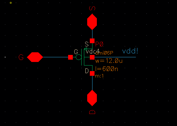
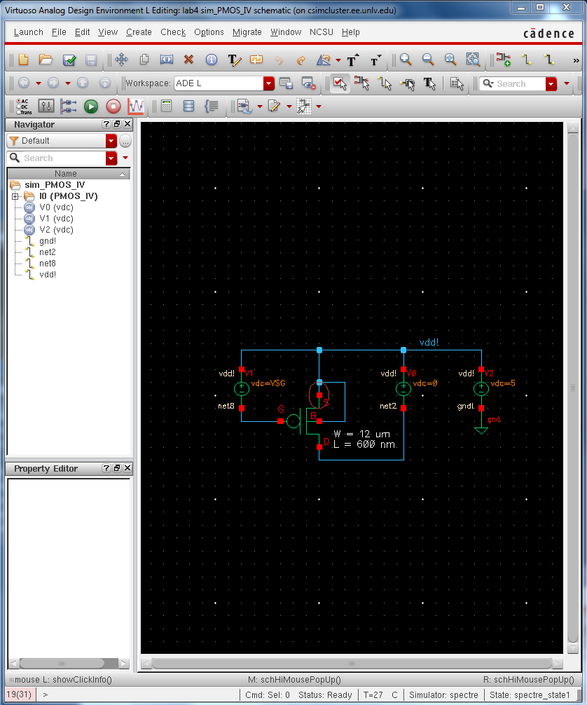
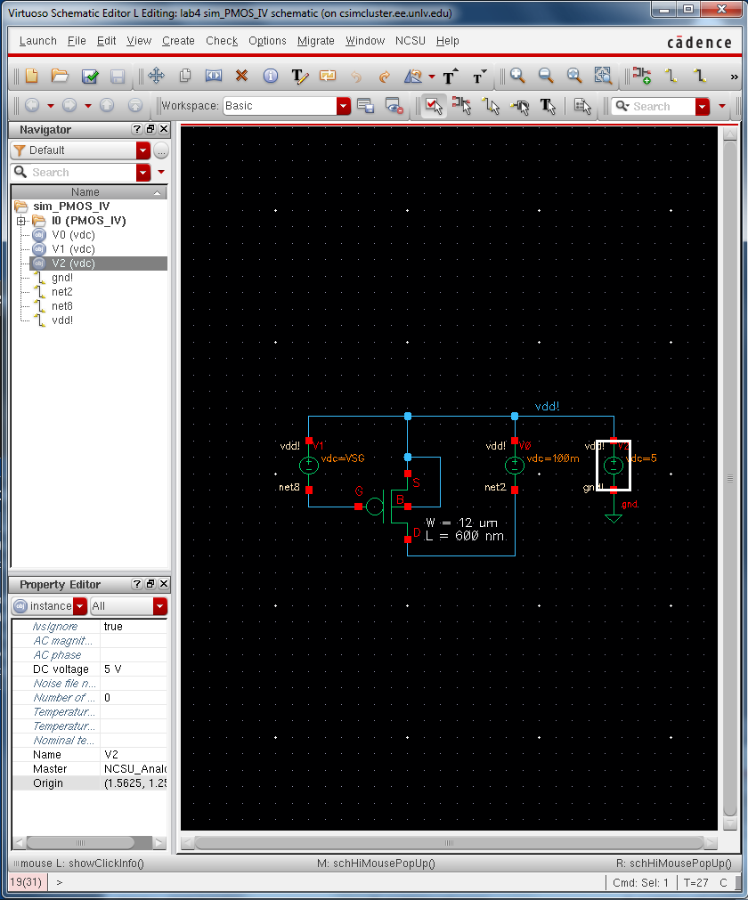
And the same process was done for PMOS except that the body is now at vdd! (global once again and this net is specificed within the schematic once again).