Lab 03 - ECE 421L
Lab 3: In this lab we will be using the 10k N-well resistor from tutorial 1 to create a layout view of our Lab 2 DAC and we will be verifying our schematic using DRC and LVS.
First,
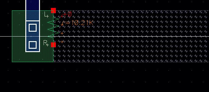
I will open and extract the Tutorial 1 10k N-well resistor to verify
it's resistance. In the C5 process the N-well resistance is about
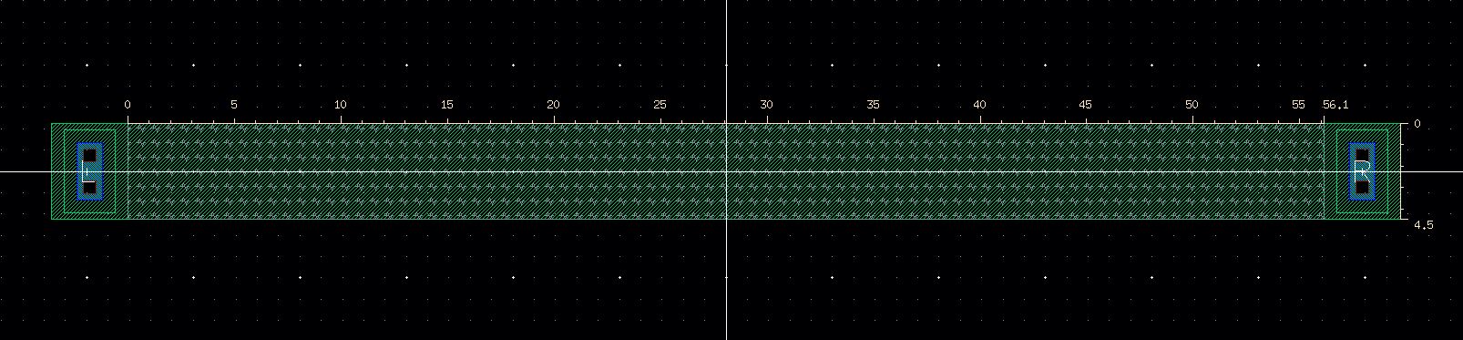
800ohms and the minimum N-well width is 12 lambda (each lambda being
300nm) which leaves us at a size of 4.5um X 56um. However, since our
DRC rules force us to go to whole numbers (divide the numbers by .15)
we must use 56.1um to ensure that it is a round number
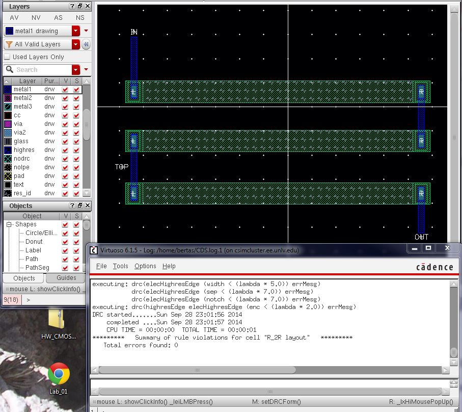
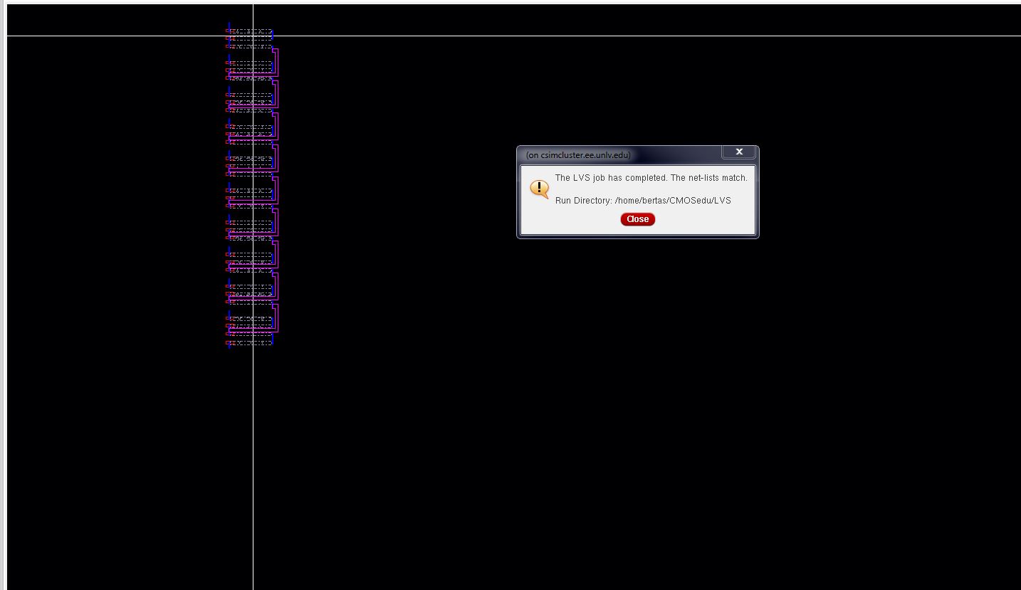
Next we know from the previous lab that our DAC is created by 10 R_2R blocks, so we should start off by creating an R_2R layout view that will allow us to quickly create our DAC. We will use this block by creating 10 instances (1 for each bit)
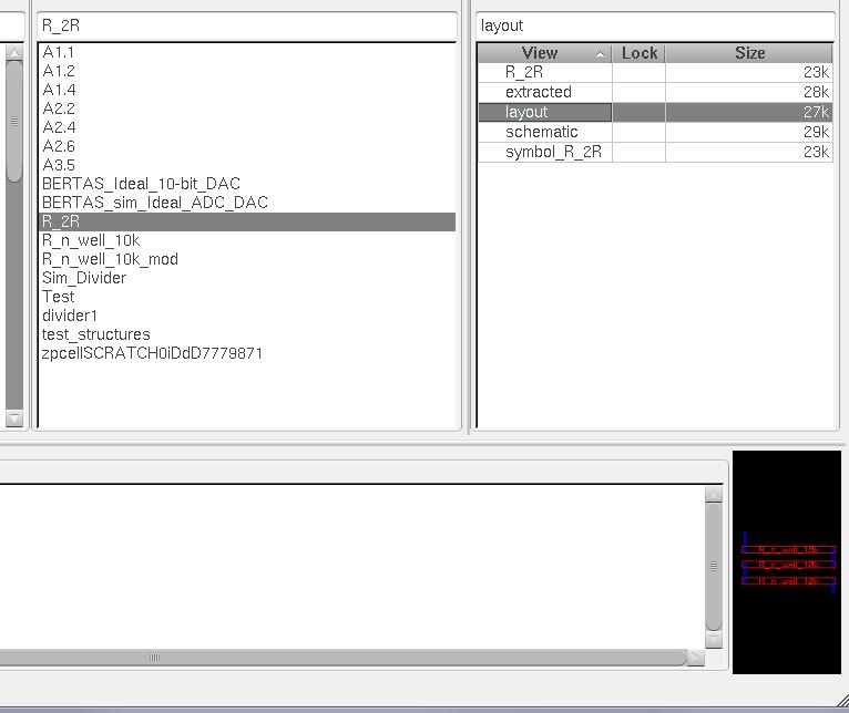
After creating the layout view we need to DRC the layout then extract it and LVS the extracted view and the schematic view (when doing the layout the pin names and I/O settings must match).
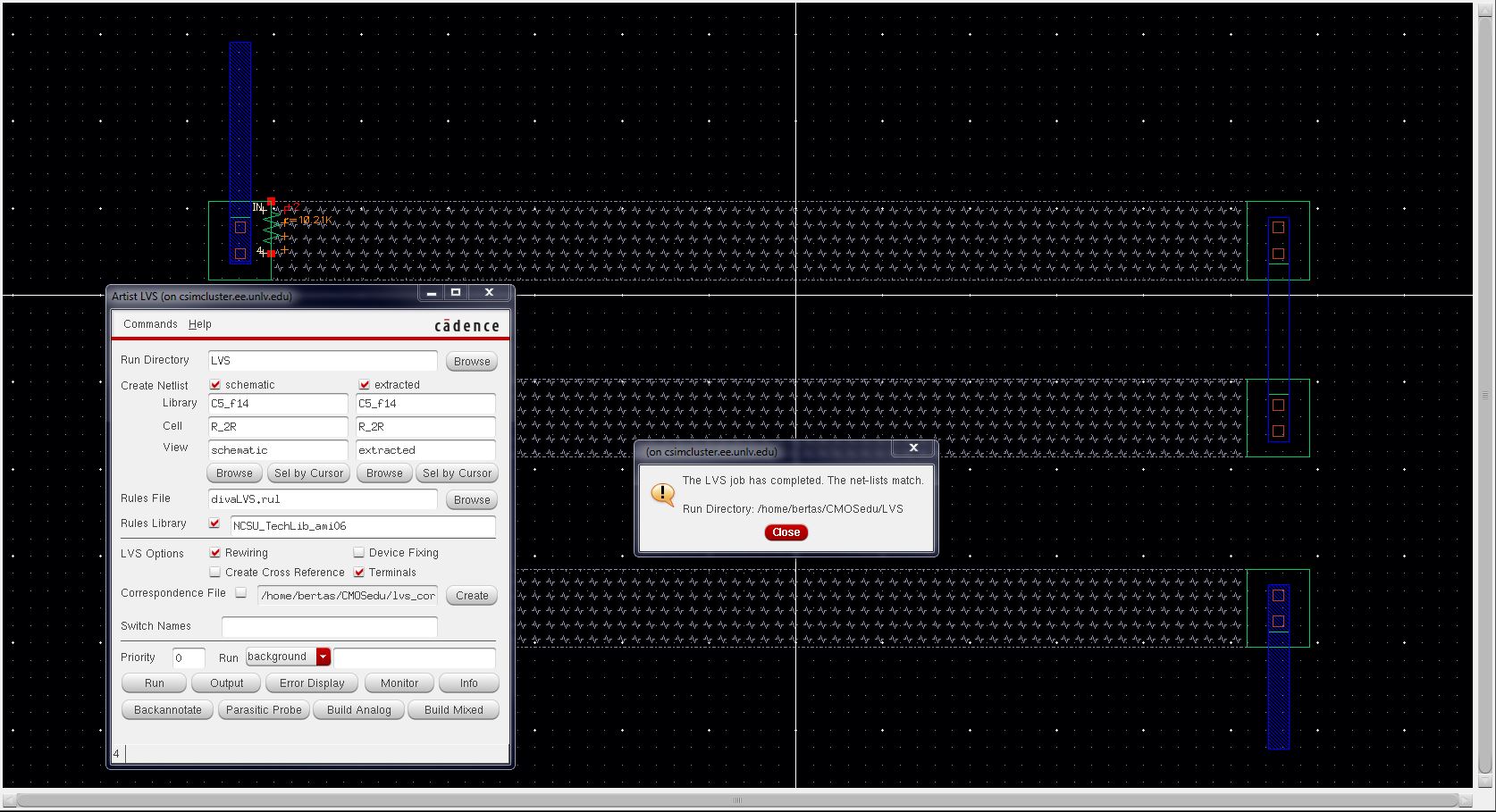
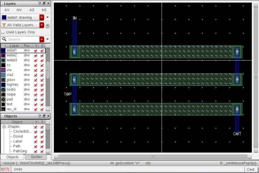
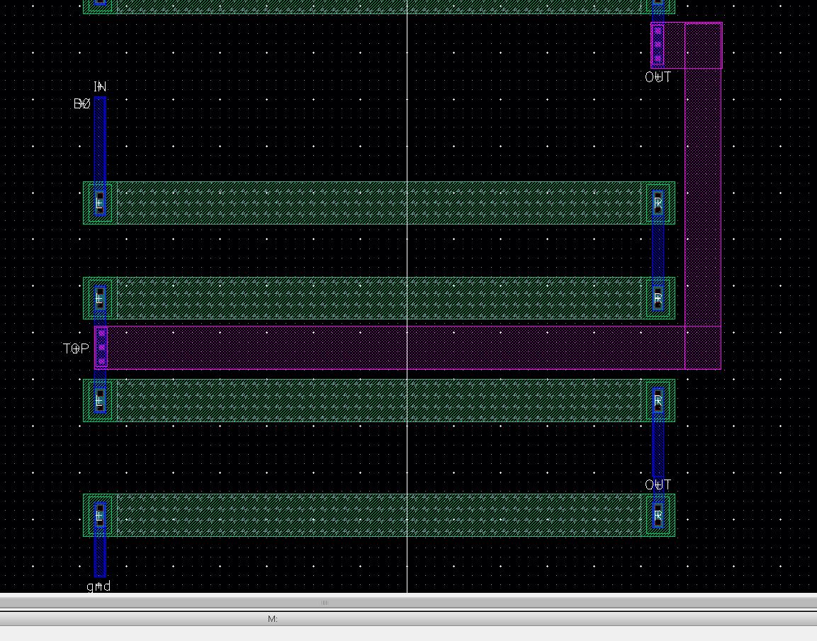
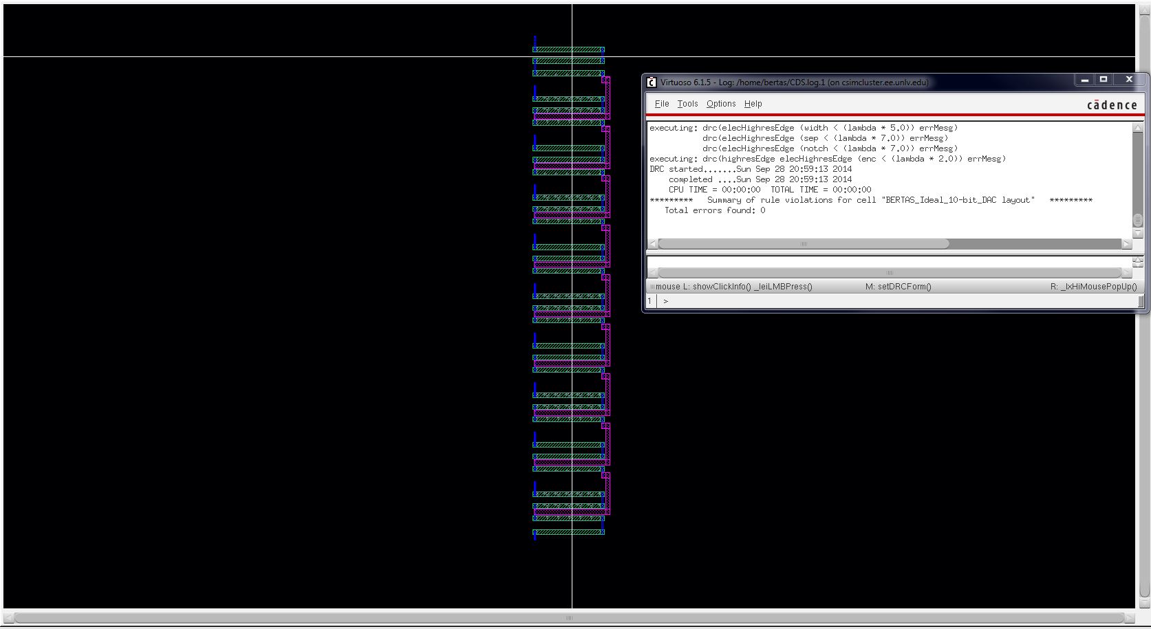
After you have verified the R_2R layout we can now instantiate it into the DAC layout (created from the library manager) and connect the pins (on metal1) using metal2/via thus leaving metal1 for the I/O terminals. We will then need to instantiate one more 10k N-well resistor for the ground output as is done in the schematic. After this we will DRC the layout and LVS it with the schematic view to ensure that we designed it correctly.
Followed by the DRC and LVS.
The zipped up files can be found HERE.