Lab 02 - ECE 421L
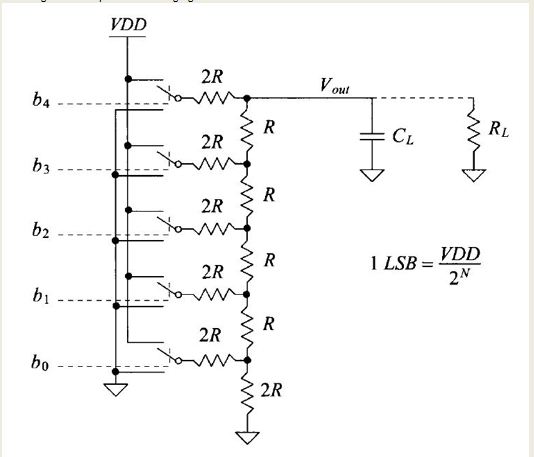
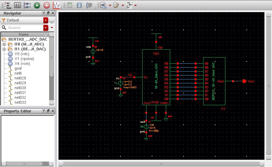
Lab 2: For Lab 2 we were tasked with creating a 10 bit DAC (digital analog converter) using resistors based on the schematic below.
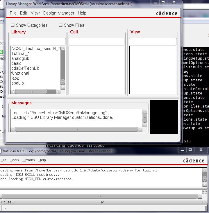
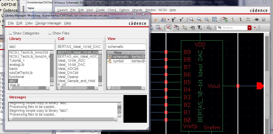
First, we needed to open the library and cell that had the working models that we would then later copy out in order to make the edits needed.
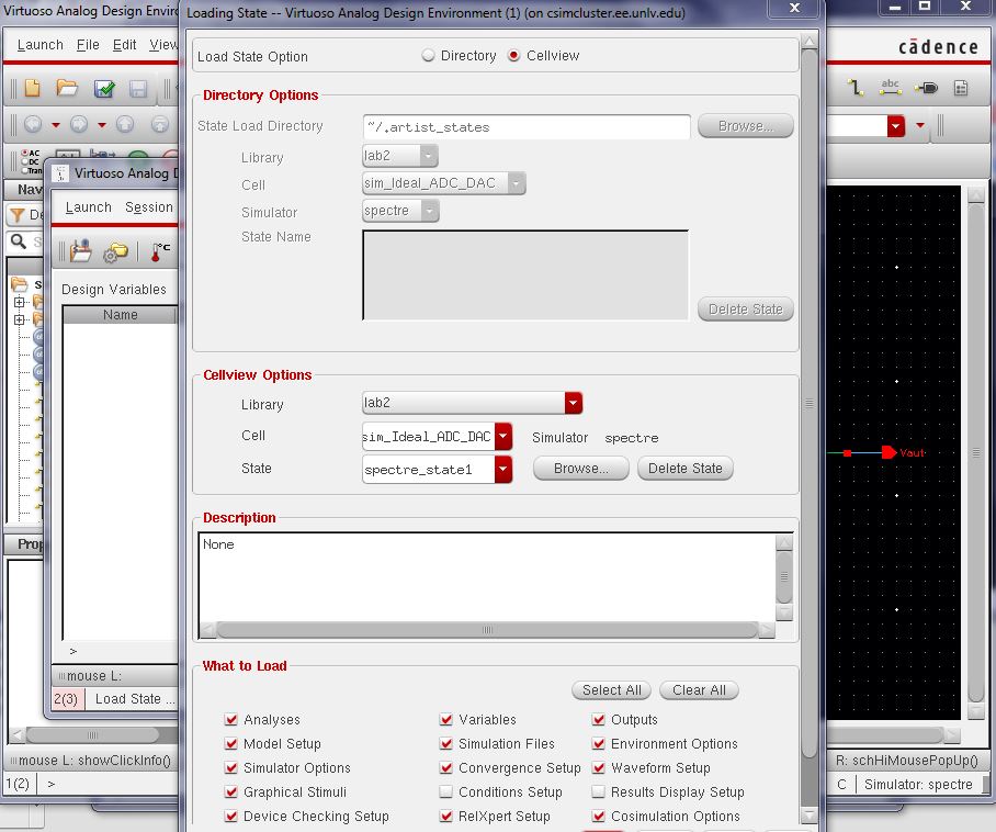
After navigating and opening the file we are opening the Analog Design Environment and loading in the state from the file to simulate it.
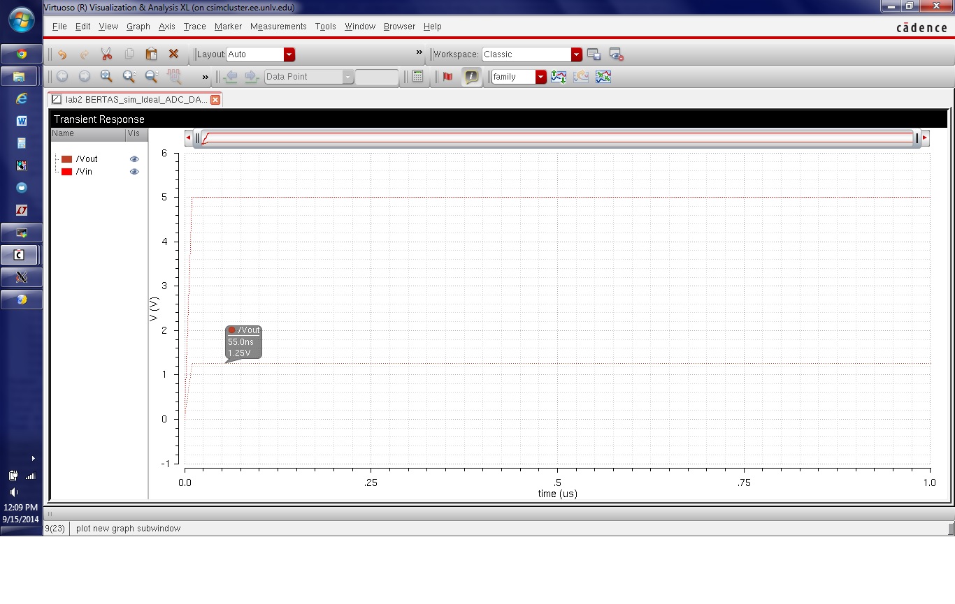
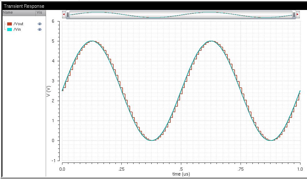
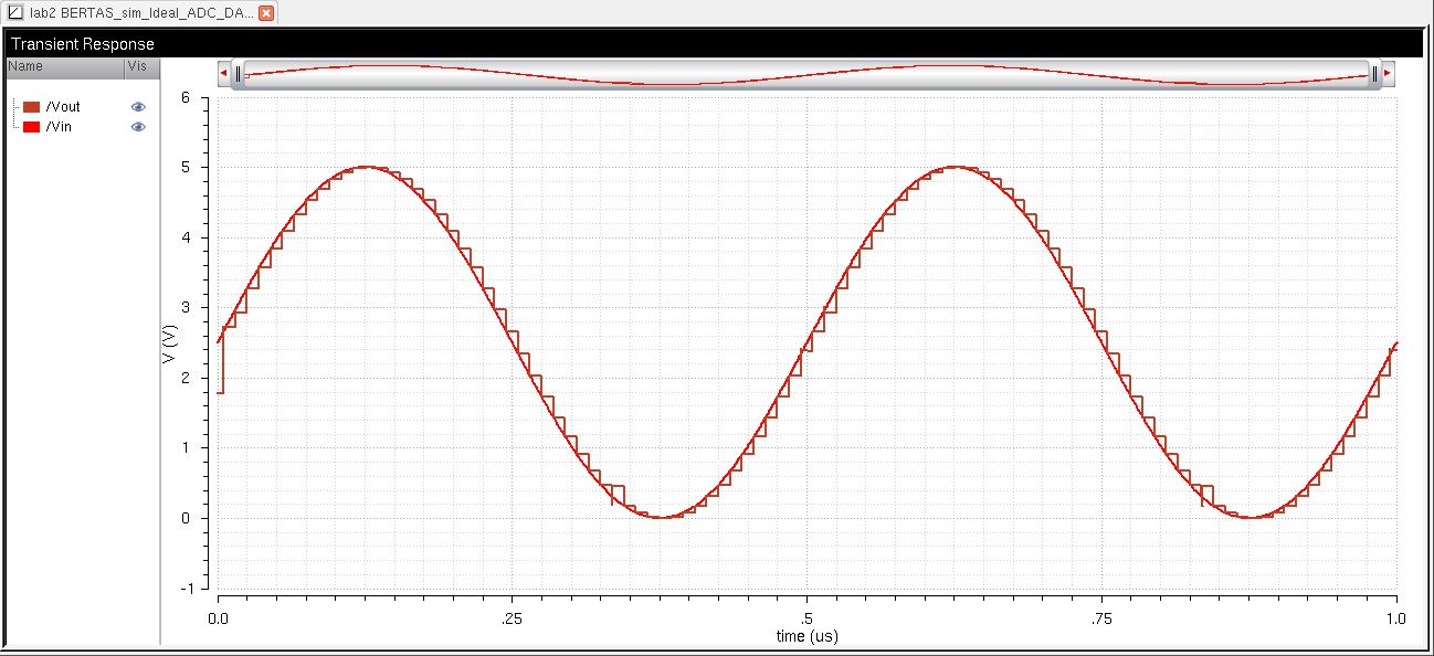
After loading the Spectre state we run a transient simulation as seen below.
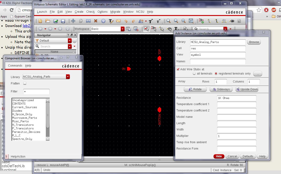
After simulating the DAC we begin to build our own using the 2R/R schematic from above. We will create 10 of these small blocks as each one will control the output for one bit. However, first we should make a copy of our working schematic so that we still have a backup file to fall back to should something go totally wrong.
Below we are setting the pins that will be shown on the block that will then be replicated 10 times (one per bit).
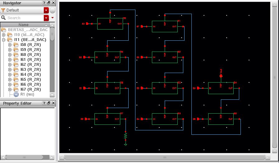
Here we can see the block on the right is the file that contains the above image, also all the pins that we have in the above schematic are shown and represented in the below overall schematic (some were deleted to match our new schematic).
Next we test our DAC using the exact same simulation specifications that we originally did to the ideal file prior to making our copy file (we simply reload the saved spectre state). We can see that the schematic matches the original exactly, meaning our DAC using resistors worked.
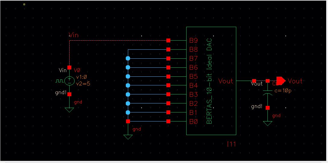
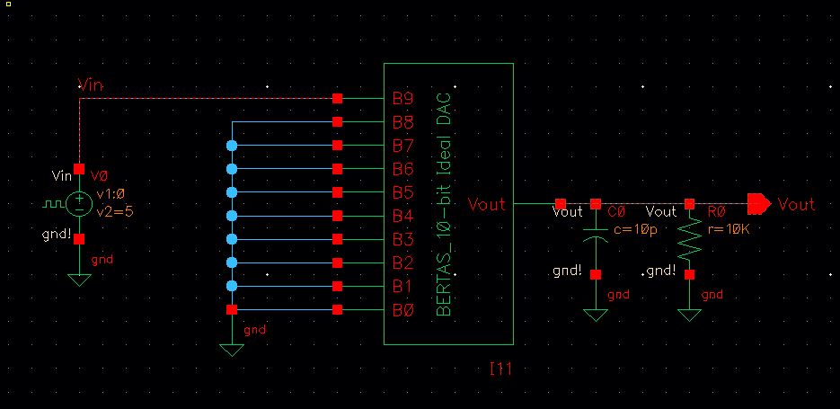
Now that we know our schematic works we will begin experimenting with some loads. Below we added a 10pF capacitance to the circuit and fed it with a 0 to 5V pulse source. As you can imagine in a transient response the output should have an RC delay (10k being equivalent resistance of our DAC). The RC delay should be right around 0.7RC and for our 10k and 10pF we can expect to see an answer being around 70ns.
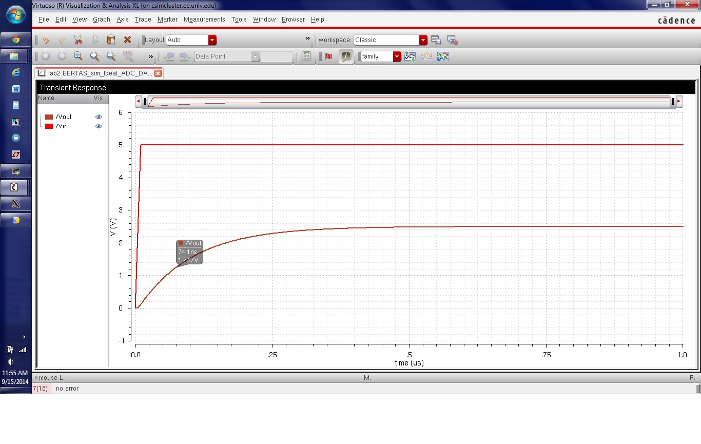
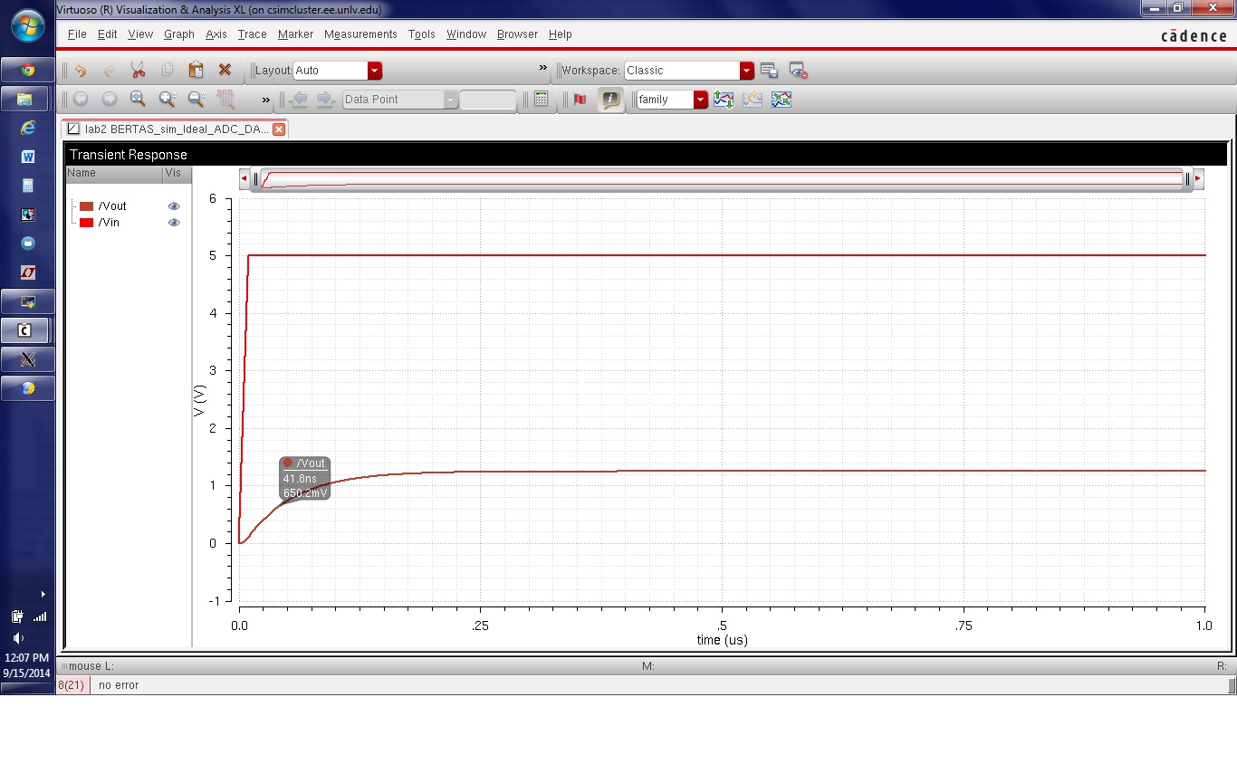
Below we see that our 70ns estimate comes out to being extremely close to the simulated value below.
Next we simulate using a load of 10pF and a 10k resistor. Based off our previous estimate it is safe to say that our Vout will be half of our previous Vout (since it now looks like a voltage divider of two equal resistors) and that we will see a shorter delay.
Our estimates are then verified below.
Next we will run this with a simple 10k load, this should only affect Vout by decreasing it to half of Vin.
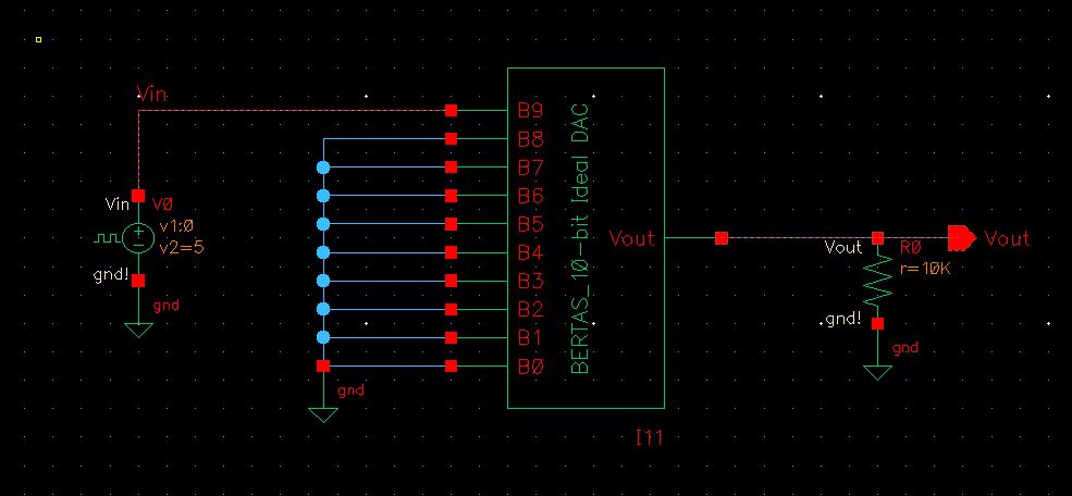
Below we can see that this is verified and that it is acting as a voltage divider.