Lab 02 - ECE 421L
Download the zip file for the lab from this link.
Create a new folder in CMOSedu named lab2. Unzip the file and upload the contents to lab2. Add DEFINE lab2 $HOME/CMOSedu/labl2 to your cds.lb file. Launch Virtuoso.
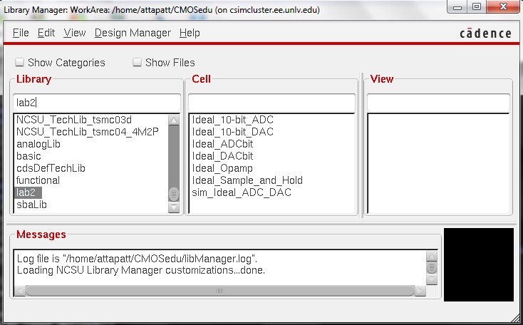
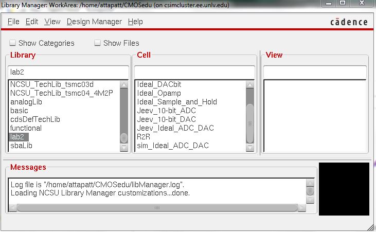
The Library manager should now show the lab2 library and its Cells.
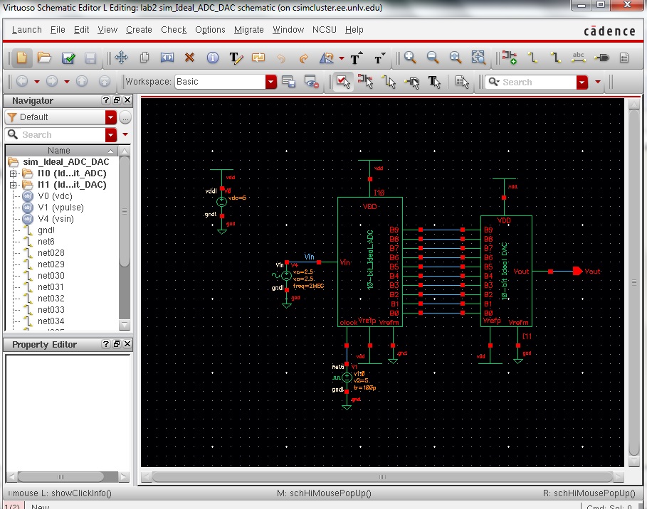
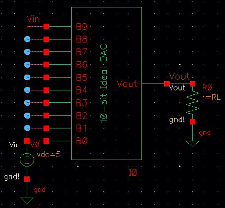
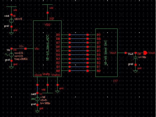
Go to the schematic of the ideal ADC DAC.
Launch ADE and load the state. The state should be a transient analysis up to 1uS and Vin and Vout slected to plot.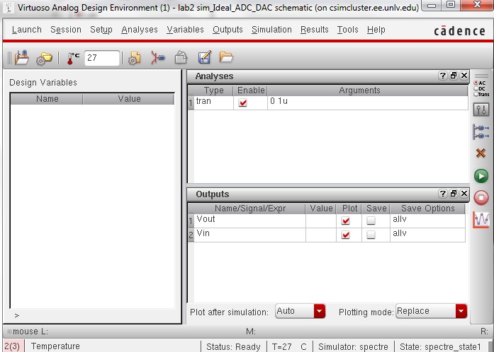
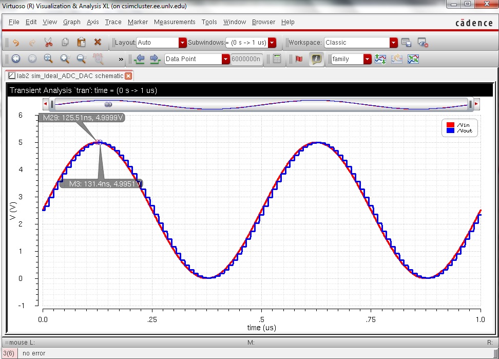
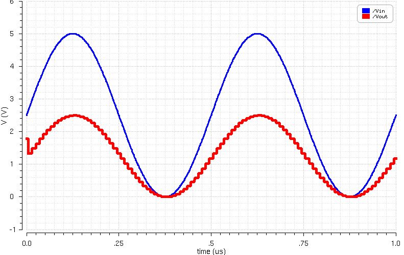
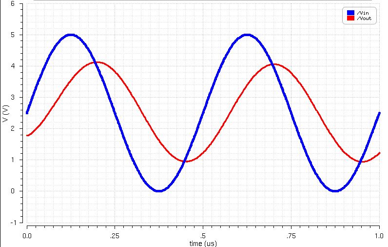
Run the simulation. You should see a smooth curve for the input voltage and a trianglular voltage for the output signal.
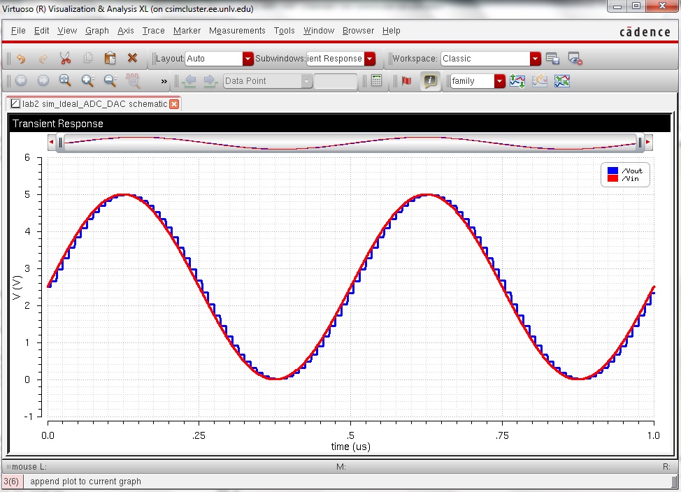
The 10bit ADC has 2^10 possible outputs. This is 1024. So if the input signal is 1V then the ADC output would be accurate up to 1/1024 of a volt.This is about 0.977mV. At 5V max 4.88mV sensitivity. At the 5V mark for the analog signal the digital signal could be 4.88mV larger or smaller. This is in fact what is seen after using some markers.
Now that we know how the ideal ADC & DAC out puts look, lets modify the DAC. First start by creating copies of the ideal versions. Right click on Ideal_sim_ADC_DAC & Ideal_10-bit_DAC. Click copy to create new versions for editing.
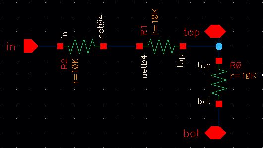
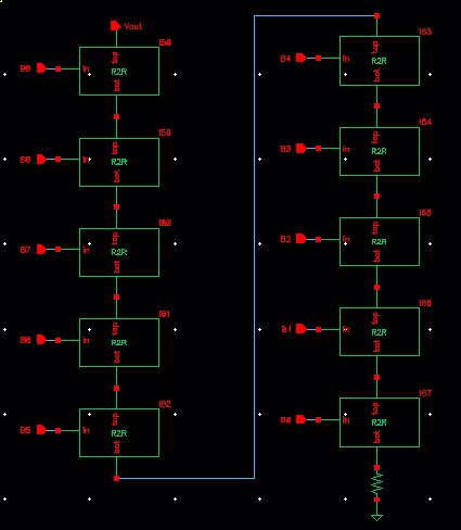
From the Library manager go file->new->cell view. Create a new cell view schematic called R2R. This will be your 1-bit DAC. It should be similar to the layout below. Use 10K resistors only.
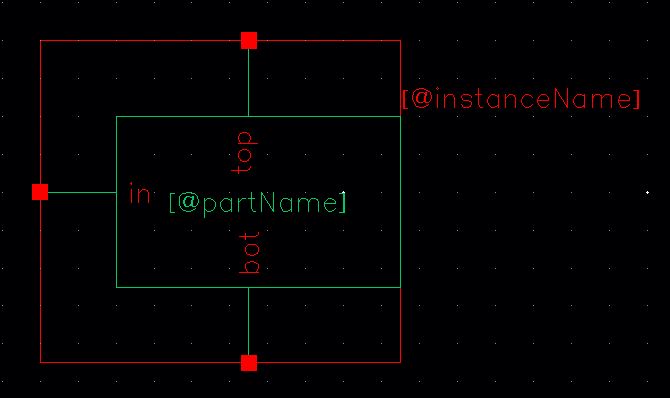
Go to create->cell view->from cell view. This will create a symbol to use in your 10-bit DAC.
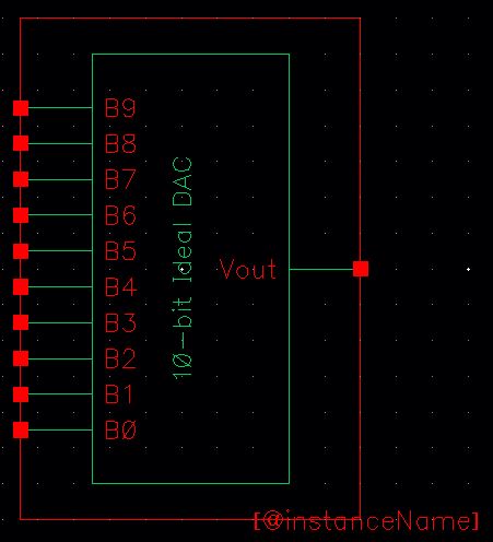
Go to the new copy of the 10 bit DAC and modify it. Replace all the 1bit DAC with the ones just created. The new circuit schematic and symbol should be similar to the images below.
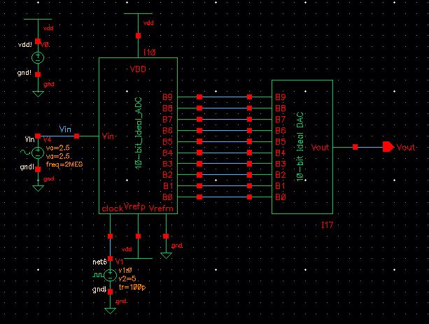
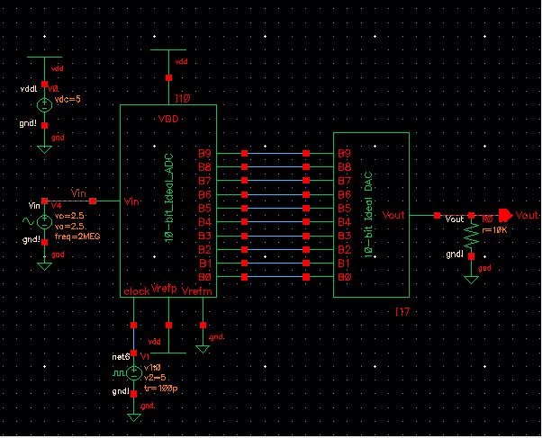
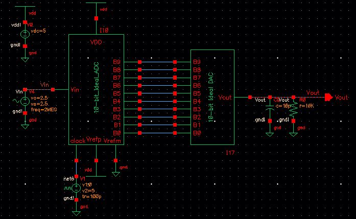
Now we will be doing simulations on the new DAC. Go to your copy of the ADC DAC circuit. Replace the ideal DAC with the new one. Notice the fewer pins on the DAC of the new schematic.
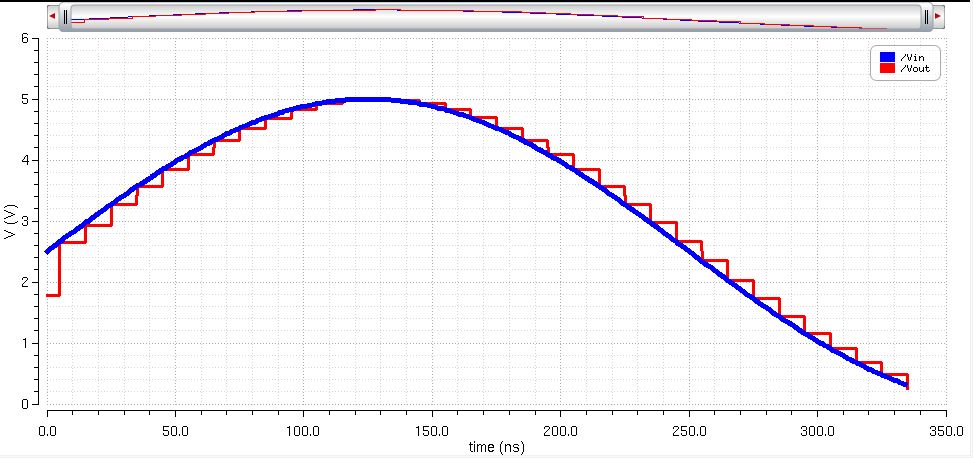
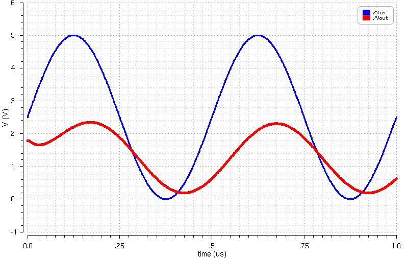
Run the transient simulation for 1us. The image below shows that there is still an analog to digital to analog conversion occuring.
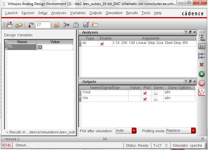
The next step is determining the out put resistance. To do this I have chosen a parametric sweep. First set up the the circuit schemtic below. Make sure that the resistor is set as RL. Then in the ADL choose the parameters as shown below.
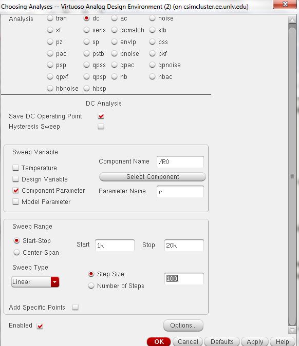
The ADL window should appear as below. The 1k resistance assigned to RL is to initialize the resistor.
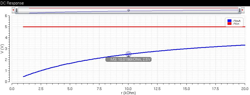
The resistance where the output is half the input is the output resistance. When Rout=RL then we have a 2:1 voltage divider. As can be seen from the graph below the Vin=Vout/2 value is about 10k. Therefore Rout is 10k.
For the hand calculations lets take a 1bit DAC. The input pin has 2R and this goes through another 2R. From the output each 2R is in paralell. This combines to R. If a 2bit DAC the MSB has 2R. There is another R before going to the LSB. The LSB as proven previously is R. Combine the 2R from MSB with the LSB and connecting R and we get R. By induction this can be used for the 10bit DAC.
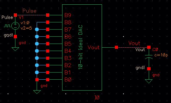
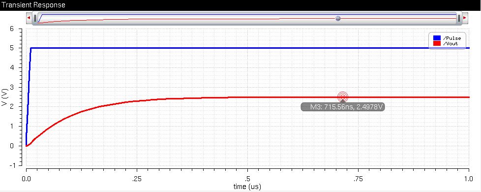
Next we have to show that the time taken to reach Vin/2 is 0.7RC. To do this set the schematic as below. We will only need one bit for this. R is Rout and C is 10pF. 0.7x10kx10p=0.7us. As the in put is 5V we must look for the location where Vout is 2.5V.
Next we attach RL then C and RL+C to the ADC DAC circuit. Attaching RL should onlt change the output magnitude. The output should be decreased by half.
Attaching C should delay the signal and decrease the amplitude. While the capacitor is signal is increasing the capacitor is charging. When the signal is decreasing the capacitor is discharging. Becuase of the ac signal some of the current escapes through the capcaitor decreasing the amplitude. The final out put is much smoother because the capacitor acts as a smoothing capacitor.
If resistance of the switches is not small compared to R then the DAC will draw more current. The input resistance of the DAC will be comparitivly less than that of the switches.