Lab 4 - ECE 421L
Lab
We will be learning how to design NMOS and PMOS transistors
Download and save C5_models.txt
Creating the NMOS transistor:
1) create a new schematic cell called NMOS_IV
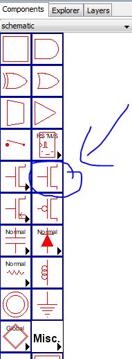
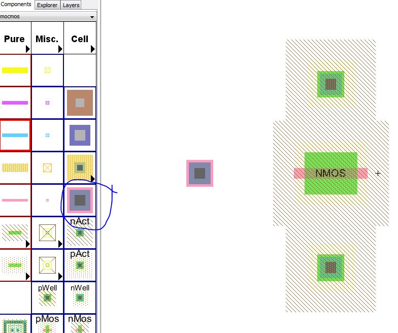
2) select the NMOS transistor from the component list in the Explorer as seen below
3) select the NMOS transistor and press ctrl+I to edit the properties of the component
4) Change the NMOS transistor width to 10 and the length to 2
5) select the NMOS transistor again and go to Tool -> Simulation(Spice) -> Set Spice Model
Spice model text should appear and change it to NMOS
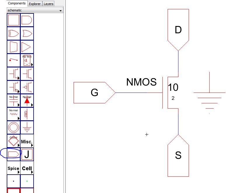
6) Place a ground component and leave it unconnected
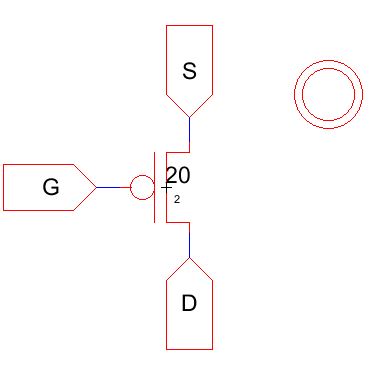
7) Create 3 pins for the terminal gates D, G and S as seen below
8) Your schematic should look like this
Building the NMOS layout
1) Create a new layout cell and name is NMOS_IV
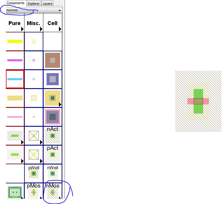
2) Place an NMOS located under components -> mocmos
3) Select the NMOS and press CTRL+I and change the width to 10 and length to 2
4) Select the NMOS and go to Tools -> Simulation (SPICE) -> Set Spice Model
5) Change the text to NMOS and CTRL+I to change the text size to 2 units
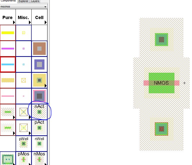
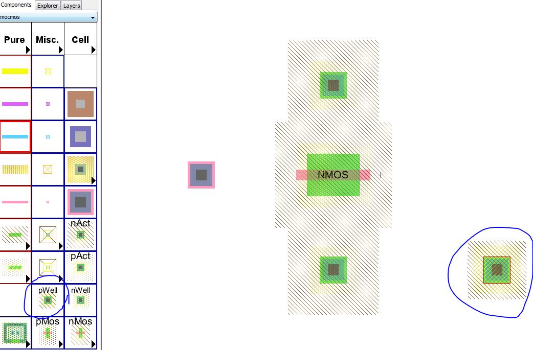
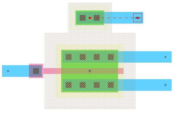
6) Select the nAct from the components explorer tab and place it above and below the NMOS
7) Add the metal1 to connect to poly1 as seen below
8) select P-well and add it to the schematic and change its width to 10 also
9) select the nAct nodes and change the X size to 10
10) select the nAct node and right click the NMOS to connect them
11) change the arc widths to 10 by CTRL+I the arc
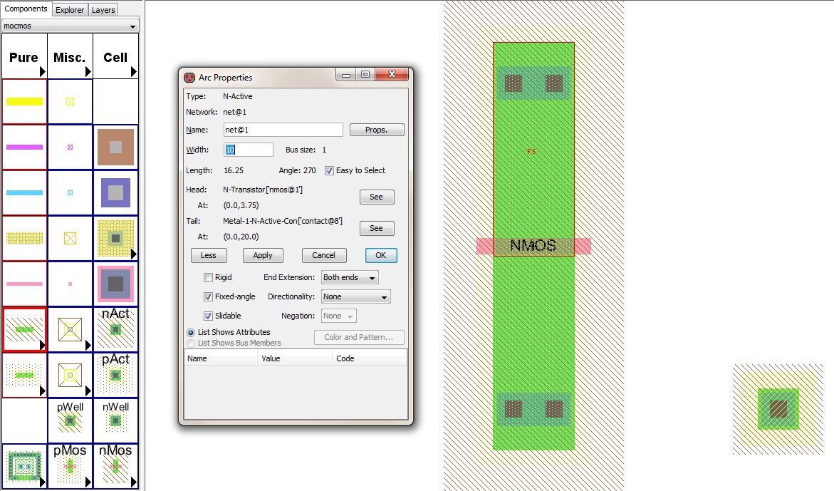
12) right click the nAct and CTRL+I and subtract about 15 units from the Y-position to ensure the minimum length between the nodes
13) connect the metal1 to the NMOS by using the metal1-to-poly connect (pink)
14) connect nodes to the terminals (g,d,s) and gnd as seen below
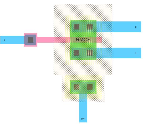
15) press F5 to see if there are any errors
Building the PMOS layout
1) The steps to building the PMOS layout is the same as the NMOS except a few things
- Use PMOS instead of NMOS
- Set the width to 20 because of the differences in mobility
- Use N-well instead of P-well and Pact instead of Nact
- The bulk/body should be connected to VDD isntead of ground
- instead of placing a ground for the NMOS, place a power node (the 2 circles in the components explorer tab)
Here is the following schematic and layout:
Making the Icons
1) Select the schematic and go to View -> Make Icon View
2) Create the icon by drawing symbols and wires to obtain the following, leave the export labels and delete everything else
NMOS
![]()
PMOS![]()
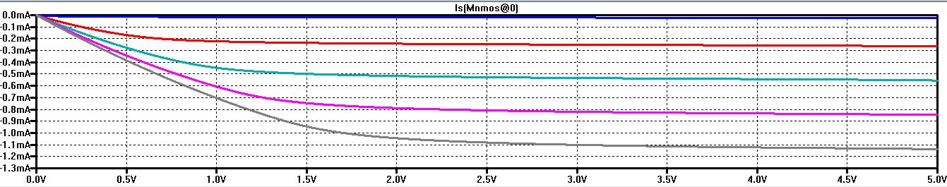
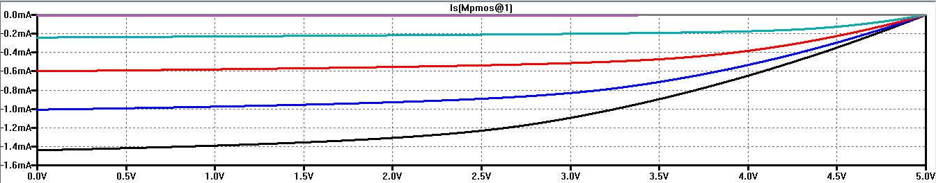
Simulations
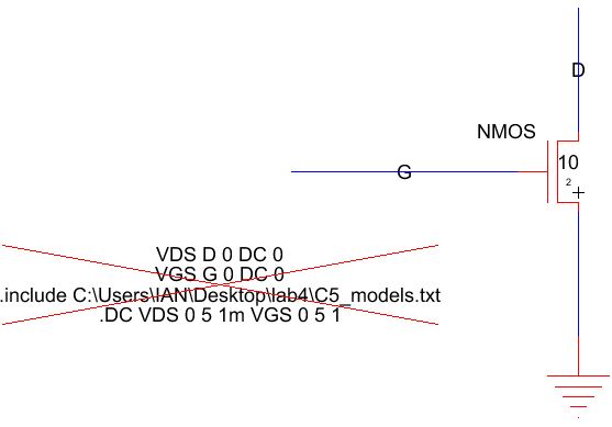
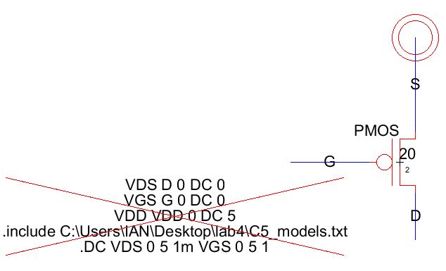
1) Duplicate both the schematic cells and name them as "sim_NMOS_IV" and "sim_PMOS_IV"
2) The schematic and SPICE code should look as below:
3) run the simulation and the following results should appear
NMOS
PMOS
The Electric Library for Lab 4 can be downloaded here LAB4