Lab 2 - ECE 421L
Ian Yanga
yangai@unlv.nevada.edu
September 6, 2013
Prelab
1) Download lab2.jelib by right clicking and Save as
2) Using Electric, open the course jelib file (ee421_ecg621.jelib) and then open lab2.jelib
3) In the Electric menu, go to Cell -> Cross-Library Copy
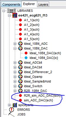
4) Copy sim_ADC_DAC{sch} and click "Copy subcells" and "Copy all related views" as seen below in the image
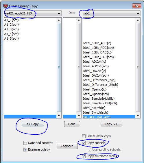
5) Click "Done" and then close the lab2.jelib in Electric's Explorer and Save by clicking on the floppy disk
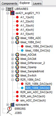
6) Run simulation of sim_ADC_DAC{sch} under the Ideal_Switch tab in Electric's Explorer as seen below
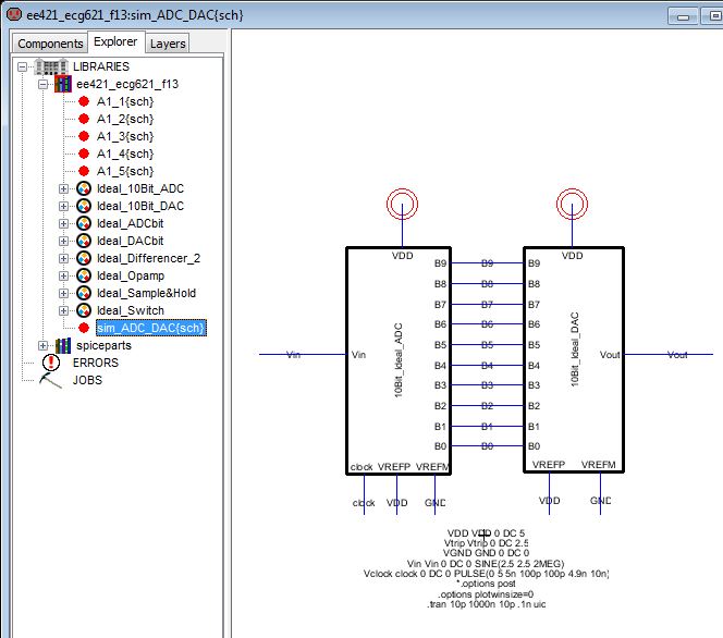
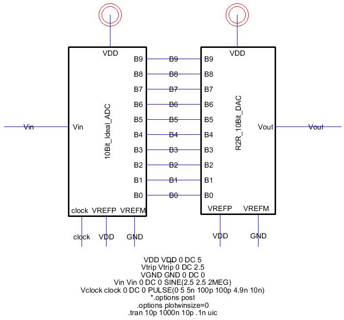
7) Run the simulation setup in the cell sim_ADC_DAC seen above to get the following below:
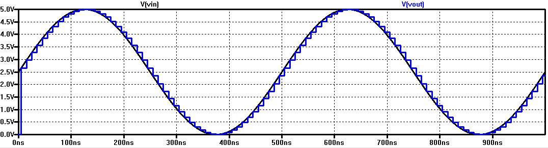
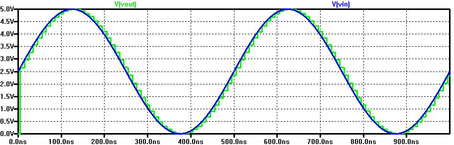
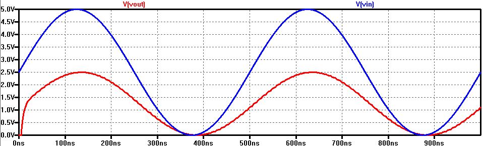
As seen in the simulation above, Vin is represented as the voltage coming into the ADC which is a smooth sinusodial wave.
Vout is the result of the DAC. The ADC converts analog signals to digital signals and then the DAC converts the digital
signal back to an analog signal which results in a step sinusodial function.
The least significant bit (LSB) is the minimum voltage change. The number of bits, n, in the converter determines the LSB value
by the equation LSB=Vref/2^n. In our example, we have n=10 bits and Vref=5v therefore:
LSB=5/2^10 => LSB=5/1024 => LSB = 0.00488 or 4.88mV
This means that the higher number of bits, the lower the LSB, the better the resolution.
**Back up all work**
_________________________________________________________________________________________________________________
Lab
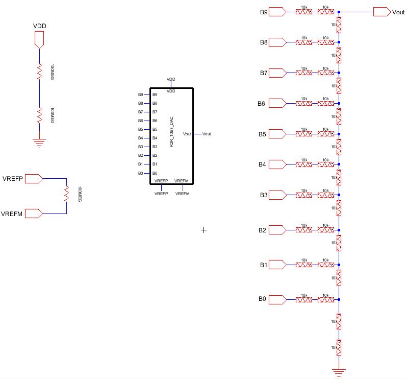
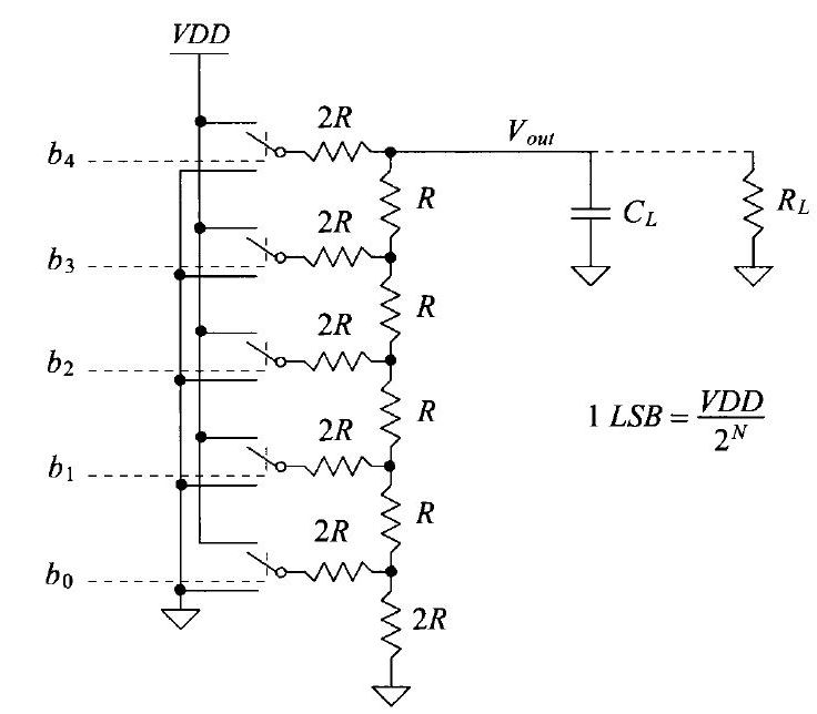
Designing a 10-bit R-2R DAC:
1)
Duplicate the Ideal_10bit_DAC cell and delete everything except
the pins, block and VDD, VREFP circuits. Then, using the n-well
resistors, design the following circuit shown below:
2) Duplicate the sim_ADC_DAC{sch} cell and name it "R2R_sim_ADC_DAC{sch}
3) Replace the Ideal DAC block with the R2R DAC block by copying the ic circuit and placing it into the sim schematic block
4) simulate the circuit to obtain the following R2R_ADC_DAC waveform
5) Compare the ideal waveform and realize that it is the same, therefore this R2R_DAC design is correct
Determining the output resistance of the DAC by combining resistors in series and parallel:
Take a look at the schematic of the DAC circuit
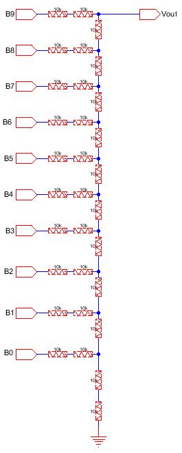
By combining the resistors, we have an output resistance of 10k.
The two 10-k resistors in series yield a resistance value of 20k which then is parallel to a 10k resistor.
When two resistors in parallel, to determine the equivalent resistance, we use the formula:
Req = (R1*R2)/(R1+R2) = (20k*20k)/(20k+20k) = 10k
Therefore the output resistance is 10k.
Delay, driving a load:
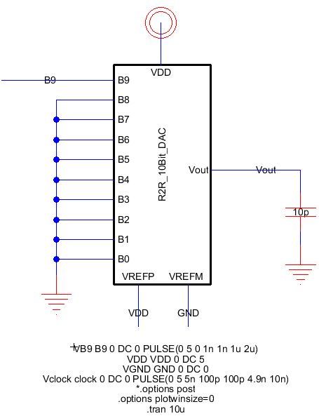
1) Duplicate the R2R_sim_ADC_DAC{sch} and name it "R2R_sim_DAC{sch}"
2) Remove everything except the R2R_10bit_DAC block
3) Ground pins B0-B8 leaving B9 alone as shown in the following:
4) Connect B9 to a pulse source from 0 to VDD
5) Connect a 10pF capacitor from Vout to GND
6) Use the following netlist:
VB9 B9 0 DC 0 PULSE(0 5 0 1n 1n 1u 2u)
VDD VDD 0 DC 5
VGND GND 0 DC 0
Vclock clock 0 DC 0 PULSE(0 5 5n 100p 100p 4.9n 10n)
*.options post
.options plotwinsize=0
.tran 10u
7) The schematic and netlist should be the following:
8) Simulate and obtain the following waveform
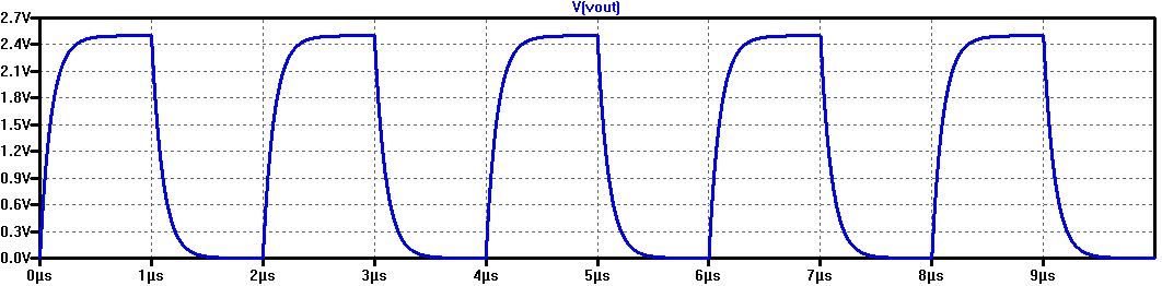
9) Let's take a closer look at one wave and determine the time delay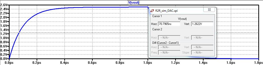
10) The time delay is calculated using the formula:
Time delay = 0.7RC where R=10k and and C=1pF
Substituting in the values, we obtain
Time delay = 0.7(10^3)(10^-12) = 7e10^-10 = 70e10^-9 = 70 nanoseconds
So when Vout is at 1.25 volts, the time delay it took to reach that voltage is 70 nanoseconds
Resistance Load:
1) Duplicate the R2R_ADC_DAC{sch} and name it R2R_ADC_DAC_resistance_load{sch}
2) Add a resistor of 10k from Vout to GND as seen in the following:
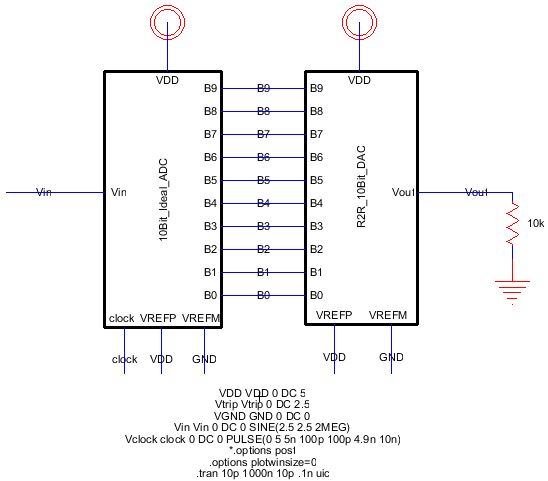
3) Simulate to obtain the following waveform
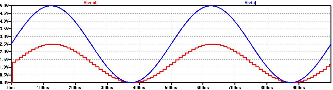
4) Vout will be half the amplitude of Vin because of the 10k resistance load
Capacitance Load:
1) Duplicate the R2R_ADC_DAC{sch} and name it R2R_ADC_DAC_capacitance_load{sch}
2) Add a capacitor of 1pF from Vout to GND as shown in the following:
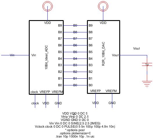
3) Simulate to obtain the following:
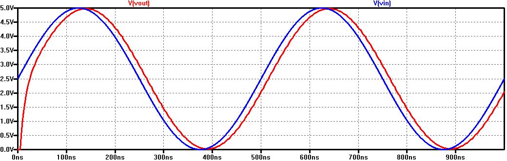
4) Vout will be the same as Vin but with a phase shift because of the capacitor and it will not have an
amplitude change because there is no resistor to change the value from Vin to Vout
Resistance and Capacitance Load in parallel:
1) Duplicate the R2R_ADC_DAC{sch} and name it R2R_ADC_DAC_RC_load{sch}
2) Add a resistor of 10k in parallel with a capacitor of 1pF from Vout to GND as shown in the following:
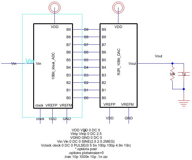
3) Simulate to obtain the following:
4) Vout will have a slight phase shift because of the capactiro and an amplitude change of half of Vin because of
the resistor, 10k.
In a real circuit, the switches seen above (the outputs of the ADC) are implemented with
transistors (MOSFETS), what happens if the resistance of the switches isn't small
compared to R.
- The output voltage will go down because the transistors because their will be a voltage drop across
the switches
Save and backup all files!Return to EE 421L Labs