Lab 7 - EE 421L
Using buses and arrays in the design of word inverters, muxes, and high-speed adders.Authored
by Adam James Wolverton
E-Mail: Wolvert9@unlv.nevada.edu
Today's
date: 11/1/2013
Lab
description:Make a schematic for a building block useful in, for example, an ALU for inverting an 8-bit word (needed for subtraction).
Using this icon, create a simulation schematic using various capacitive loads on the output of 3 of the 8 inverters.
Create schematics and icons for an 8-bit input/output array of: NAND, NOR, AND, and OR gates.
Provide
a few simulation examples using these gates (use all four of them in a
single schematic with the x8 inverter to show operation using an 8-bit
input/output bus).
Examine
the schematic of a 2-to-1 DEMUX (and the icon). Also simulate the
operation of this circuit using SPICE and explain how it works.
Can this circuit be used with Z as an input and A/B as outputs (can it be used as a MUX)? Verify using simulations.
Lab Work:
After
going through tutorial 5, I implemented the use of buses and arrays to
make 8-bit versions of an inverter, NAND, NOR, AND, and OR gates. This is seen below:
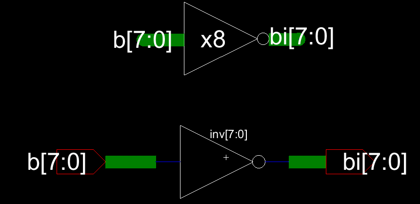
8-Bit Inverter
8-Bit NAND Gate

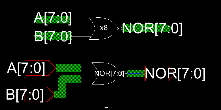
8-Bit NOR Gate
8-Bit AND Gate

8-Bit OR Gate

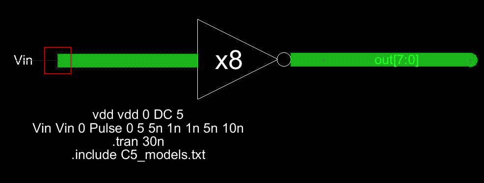
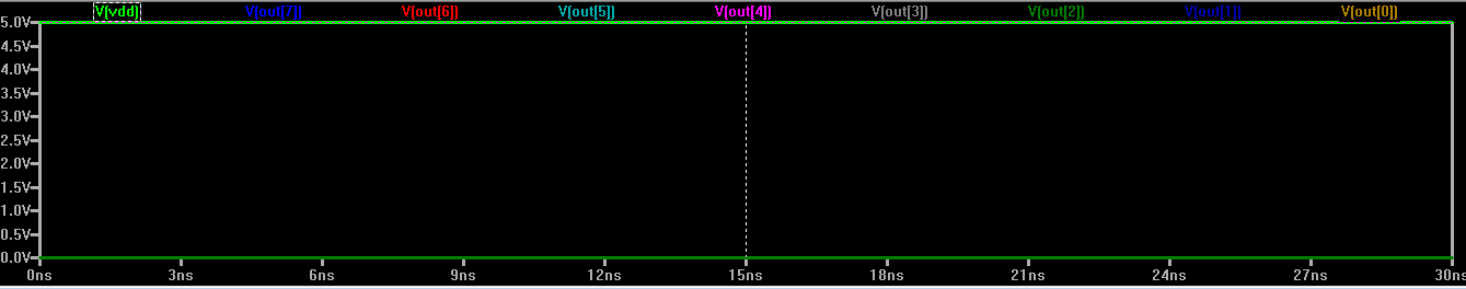
Below is the simulations for the 8-bit inverter under capacitive load and without load
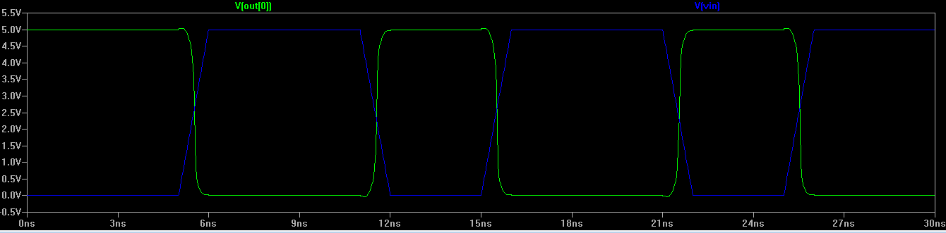


as
you can see with the varying capacitive loads, that it begins to not
keep up with the switching fast enough.
Simulating the NAND gate we get the following, which matches correct logic operation:
Simulating the NOR gate we get the following, which matches correct logic operation:

Simulating the AND gate we get the following, which matches correct logic operation:
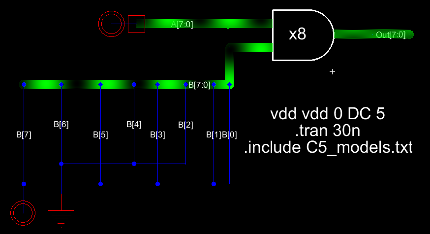

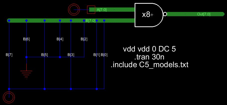
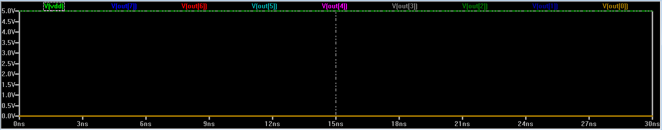
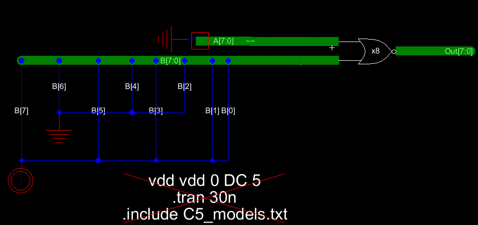
Simulating the OR gate we get the following, which matches correct logic operation: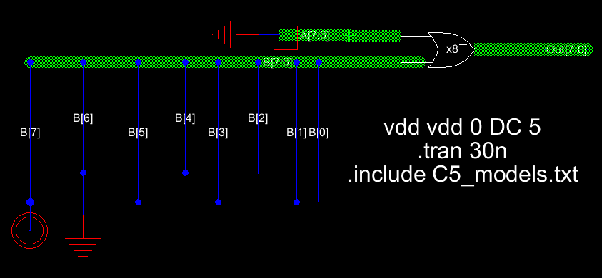
Next, I must design the schematic of the 2-to-1 DEMUX. Verify the function of the DEMUX using LTSpice.
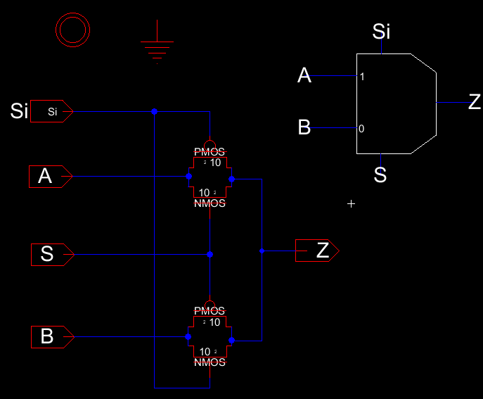
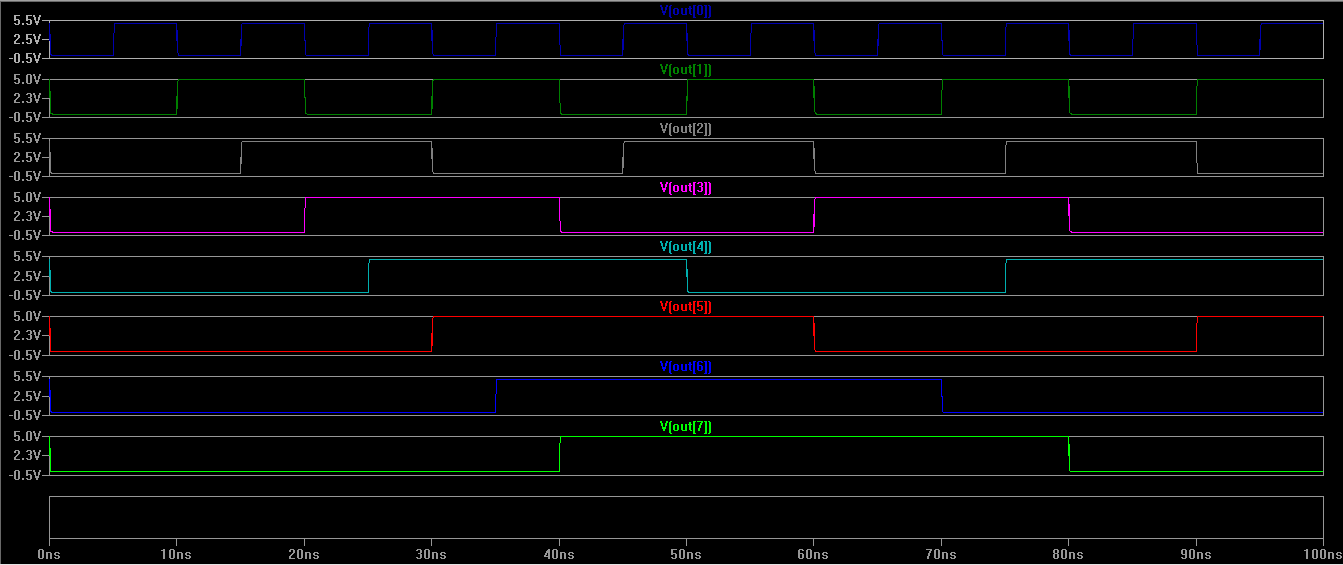
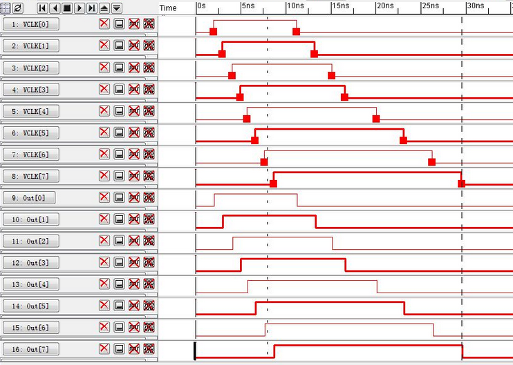
Below
are the simulations using LTSpice and IRSIM to verify that the DEMUX is
working appropriately; When the CLK is high, a high will be sent to the
output. Else, the B signal will be sent to the Z output.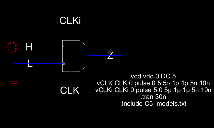


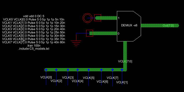
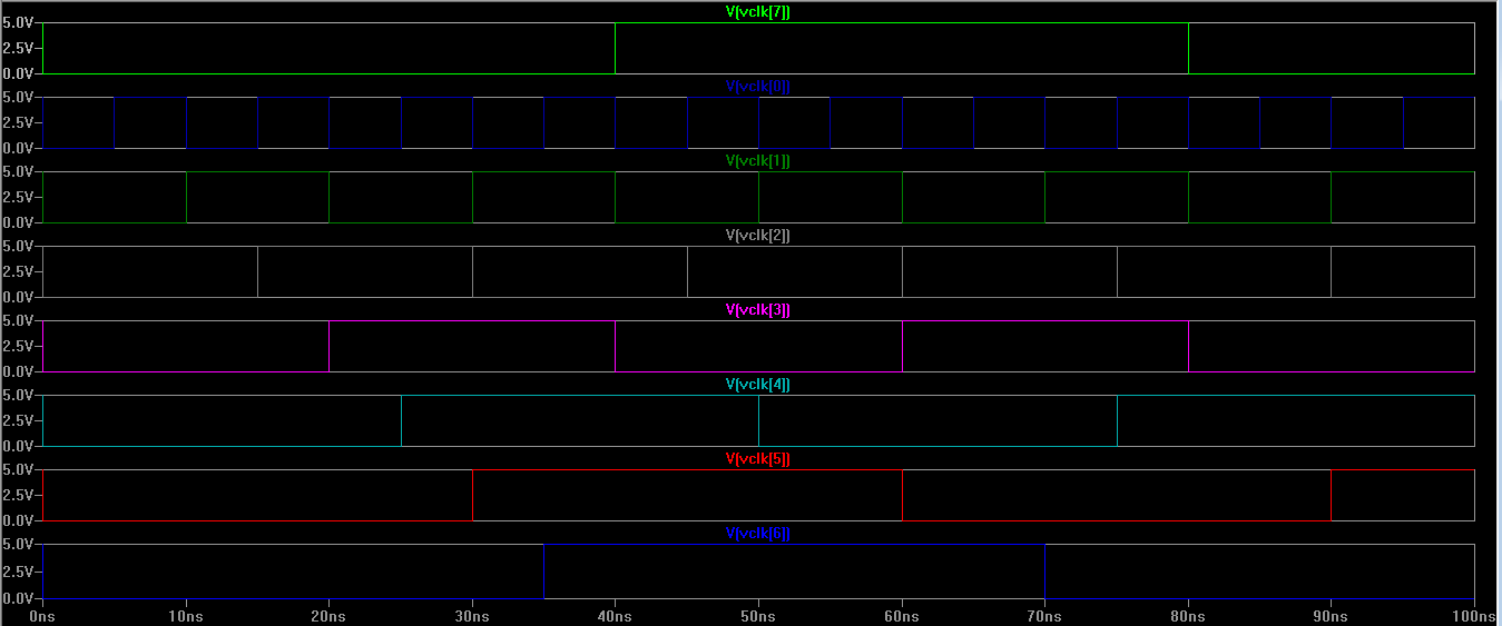
Now,
I will use a bus to design an 8-Bit DEMUX just like I did with the
gates in the previous portion of this lab. I will also verify the
circuits using LTSpice and IRSIM.

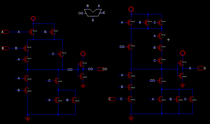
Next, part of the lab requires the design of a full-adder seen in Fig12.20 in the Textbook using 6/2 devices (both PMOS and NMOS). Also
create an Adder icon for this circuit and use this icon for a 1 bit
adder to draft an 8 bit adder schematic as well as icon. Draft the
layout after simulations.
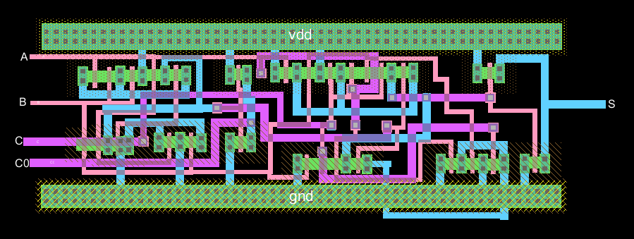

Now we work on assembling an 8bit version of the full adder by attaching 8 of the 1 bit layouts.

I couldn't get the 8bit full adder layout finished, but this is all I have.
Last but not least, I will back up my lab report as shown below:
To return to Adam's Lab directory click HERE