Lab 6 - EE 421L
Design, layout, and simulations of CMOS NAND, NOR, XOR gates and a full-adder
Authored
by Adam James Wolverton
Email: Wolvert9@unlv.nevada.edu
Today's Date: 10/13/2013
Lab
description:
1) Go through the video tutorial 4 and learn how to design schematic/layout for NAND and NOR gates.
2) Design NAND, NOR, XOR gates and use LTspice and IRSIM to simulate the gates operation.
3)Once
the gates have been designed use them to make a full-adder consisting
of two XORs, two NANDs, one NOR and three inverters. Also create a
full-adder implemented by 3 NANDs and 2 XORs.
4) Once lab is completed, back up the lab report and uplaod it to CMOSedu.com for future study and discussion.
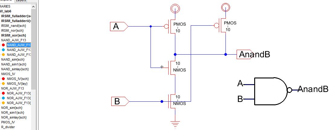
Here is my drafted schematic along with its icon of a 2-input NAND gate using 10/2 MOSFETS
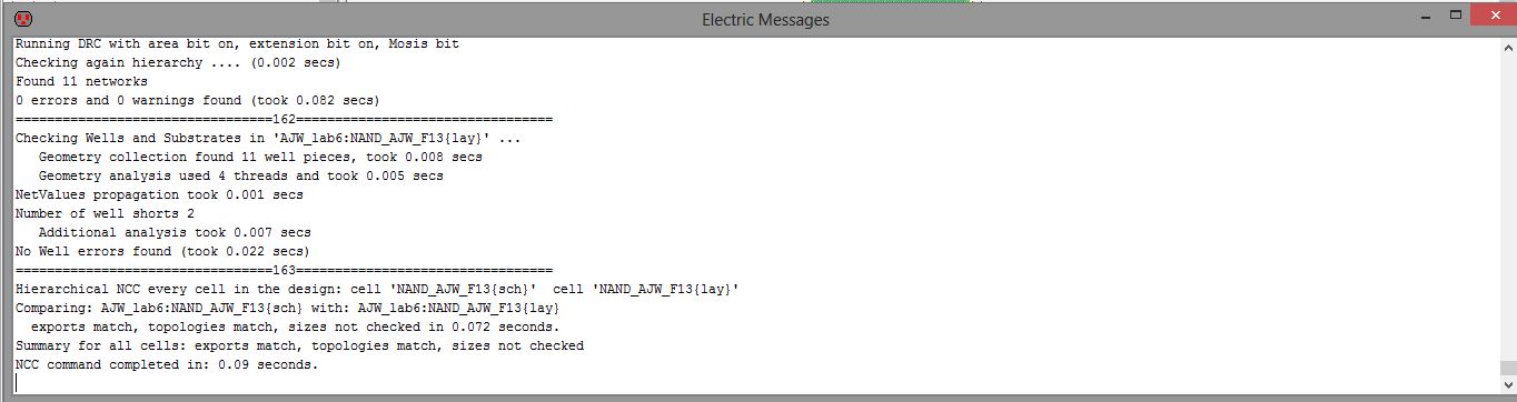
Here
is the corresponding layout for the 2-input NAND gate, and as we can
see, there are no errors using the DRC, now well errors with ERC, and
both layout and schematic match using NCC.

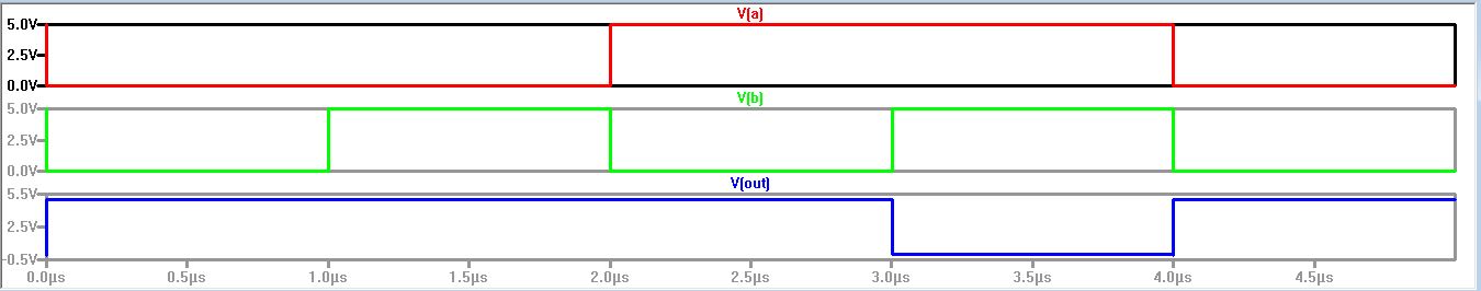
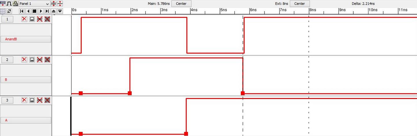
Using LTspice and IRSIM, here are the simulations of the logical operation of the gate for all 4 possible input.
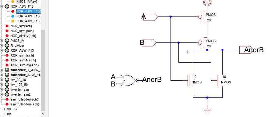
Now
to make a NOR gate, using 4 MOSFETs just like the NAND gate. This
time we will use a 20/2 sized P-Channel MOSFET. To make it easy, just
copy and change the schematic file used for the NAND gate, to avoid
tediuos work.
Below is my schematic, icon, and layout of a NOR gate:

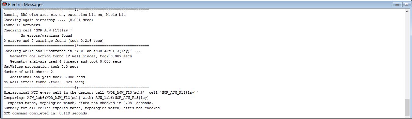
Running DRC, ERC, and NCC checked out with out any errors or mismatches as shown below:
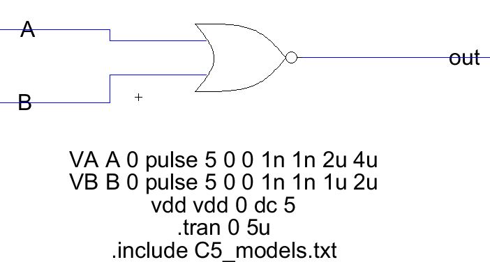
After
designing/creating the gate, lets use LTSPICE and IRSIM to verify the
gate operation. Only when both inputs are a logic 0 will the output be
a logic 1.
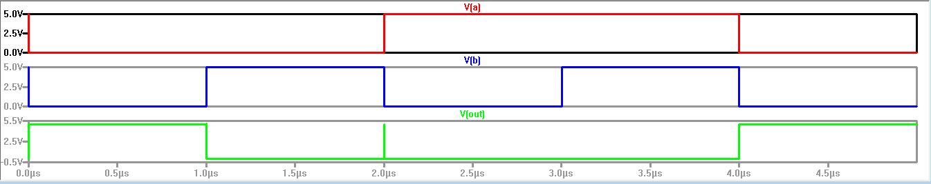
The simulations verify the correct operation of the NOR gate!
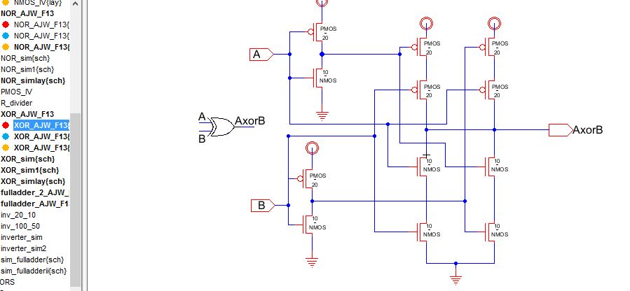
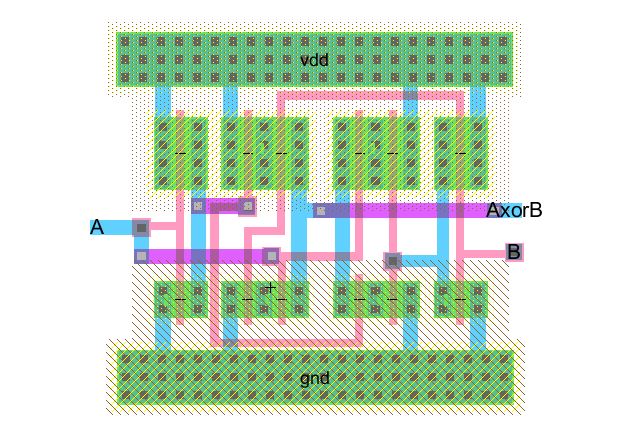
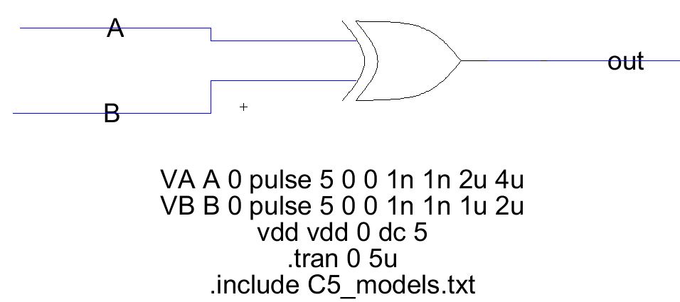
Designing
a XOR gate looking at figure 12.18 shows that the topology of this
circuit consists of two extra inverters and we have a total of 12
MOSFETs in this design of a XOR gate. Keep the NMOS size the same, but
change the PMOS to 20/10. Here is my schematic deisng, icon, and layout
of an XOR gate:
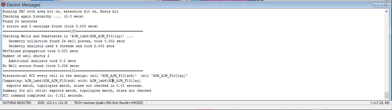
DRC, ERC, and NCC check out for the entire design of the XOR gate.
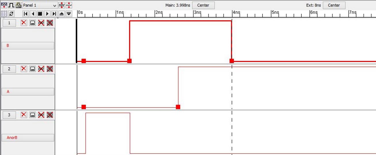
Now, let's perform verification of the gate operation using LTspice and IRSIM:
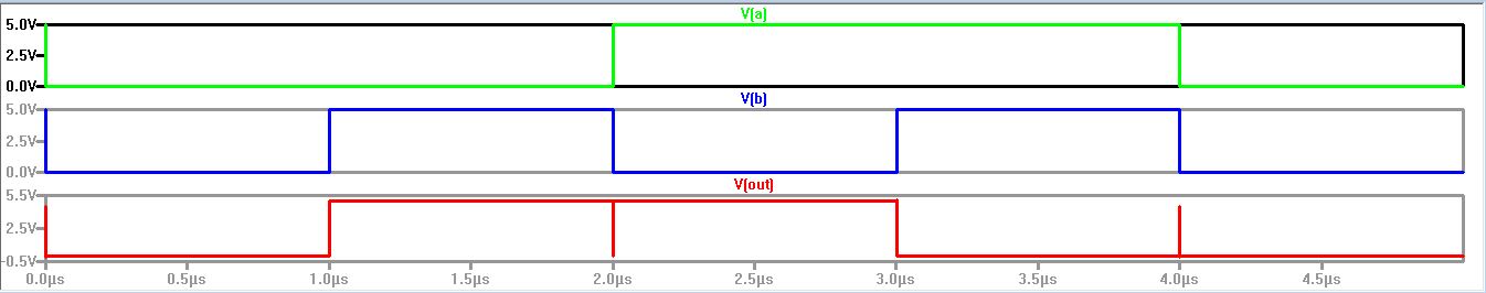
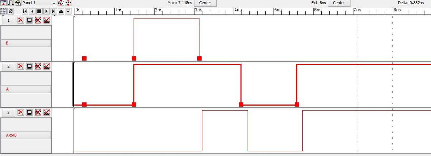
The logic checks out; the output is only a logic 1 if the inputs are different.
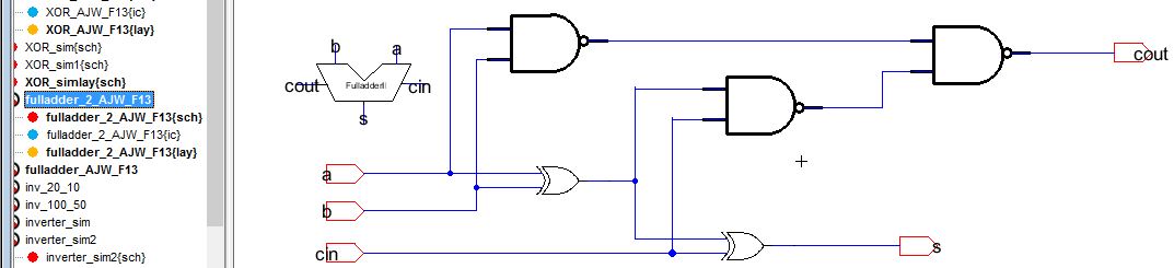
Now
we will combine what we have created in the past to design a
Full-Adder. For this first full-adder, we will use 2 NANDs, 1 NOR,
2XORs, and 3 inverters. Below is my schematic, icon, and simulations
for the described full-adder:
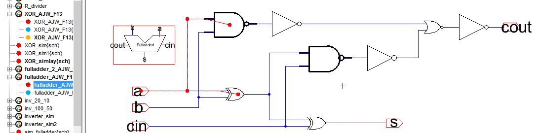
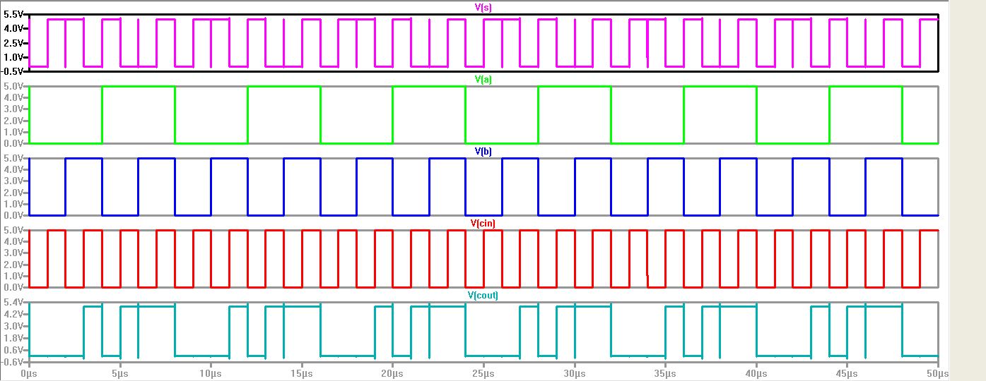
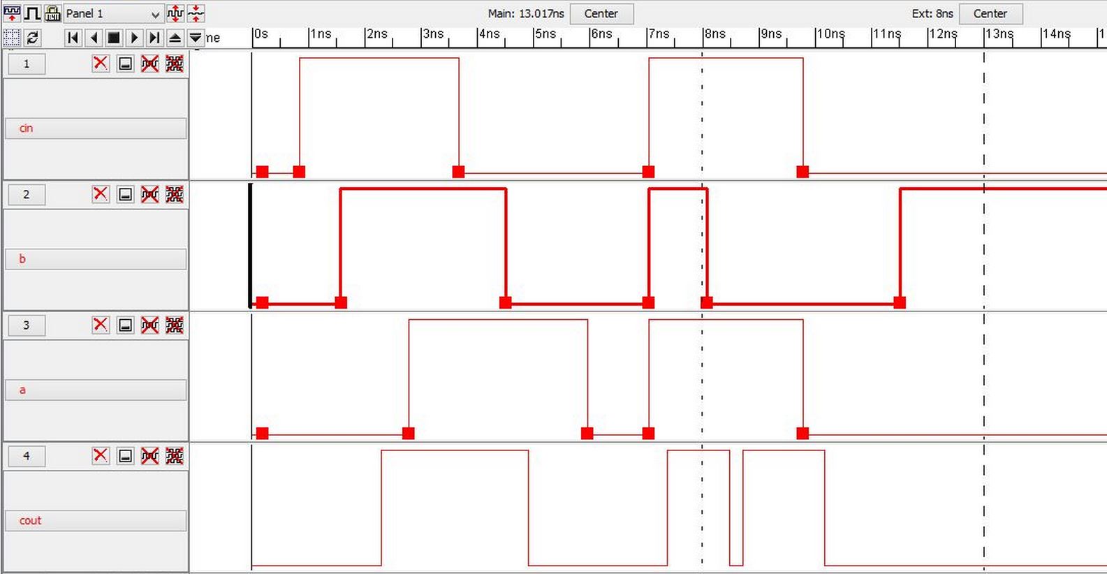
Next
is to implement another full adder with 3 NAND gates and 2 XOR gates,
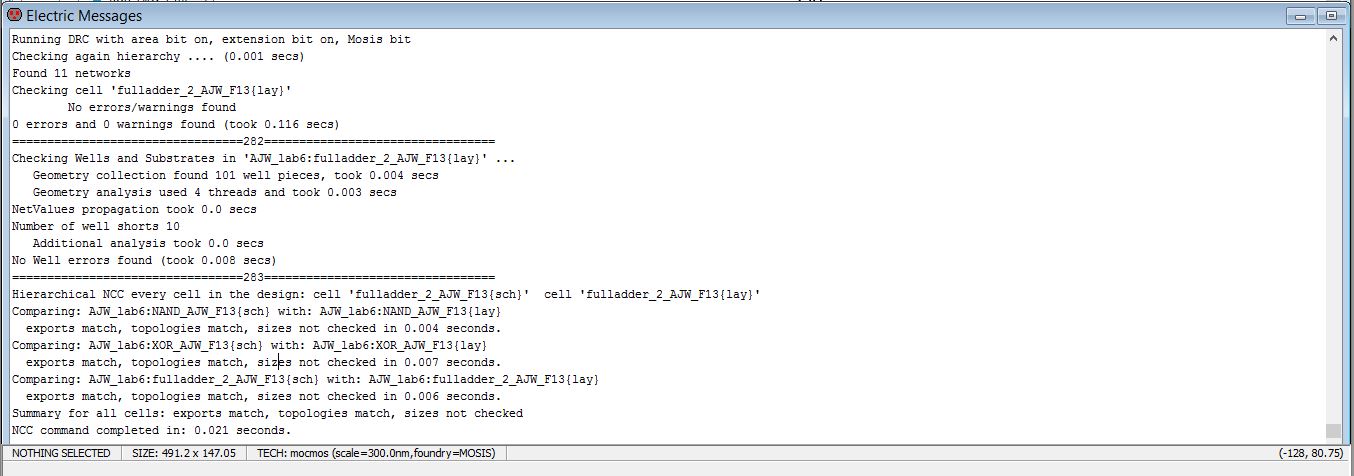
the schematic, icon, layout and all simulations are shown below:
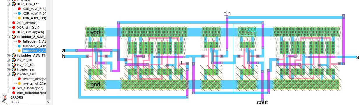
No errors from DRC, ERC, and NCC.
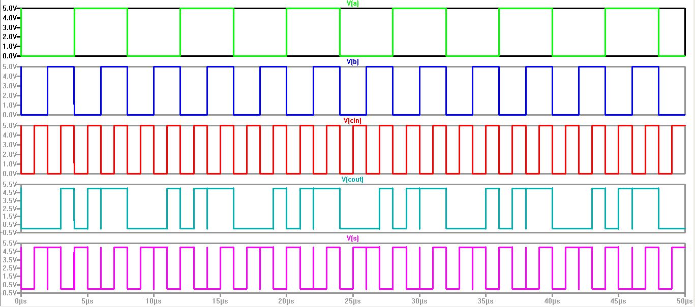
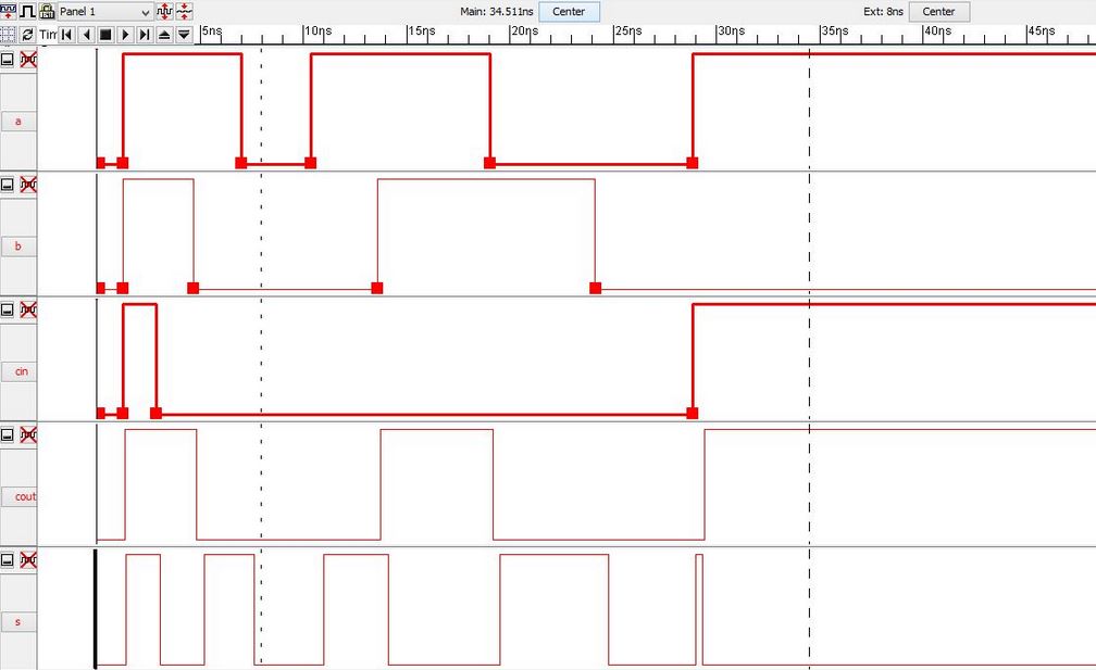
Here are the LTspice and IRSIM simulations to verify operation of the full adder:
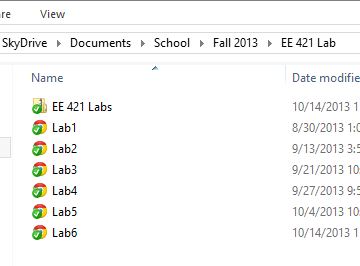
After the design is complete I backed up my lab/work as seen below:
Return to Adam Wolverton's Lab directory by clicking HERE