
Lab 5 - EE 421L
Design, layout, and simulation of a CMOS Inverter
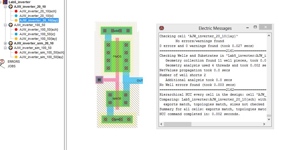
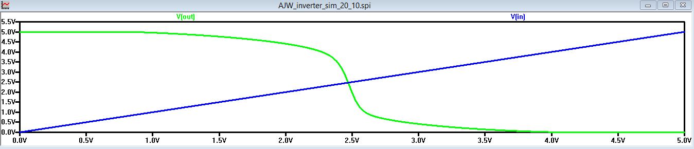
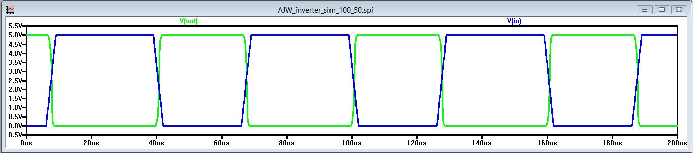
Note that I exported 4 pins (vdd, gnd, IN, and OUT) and that the PMOS is twice the width of the NMOS in order to be used together. There are no errors when running DRC, ERC, and NCC. Everything matches up. The Vout and Vin waveforms can be seen below:
Here is the schematic, icon, and layout for the 100/50 CMOS Inverter:

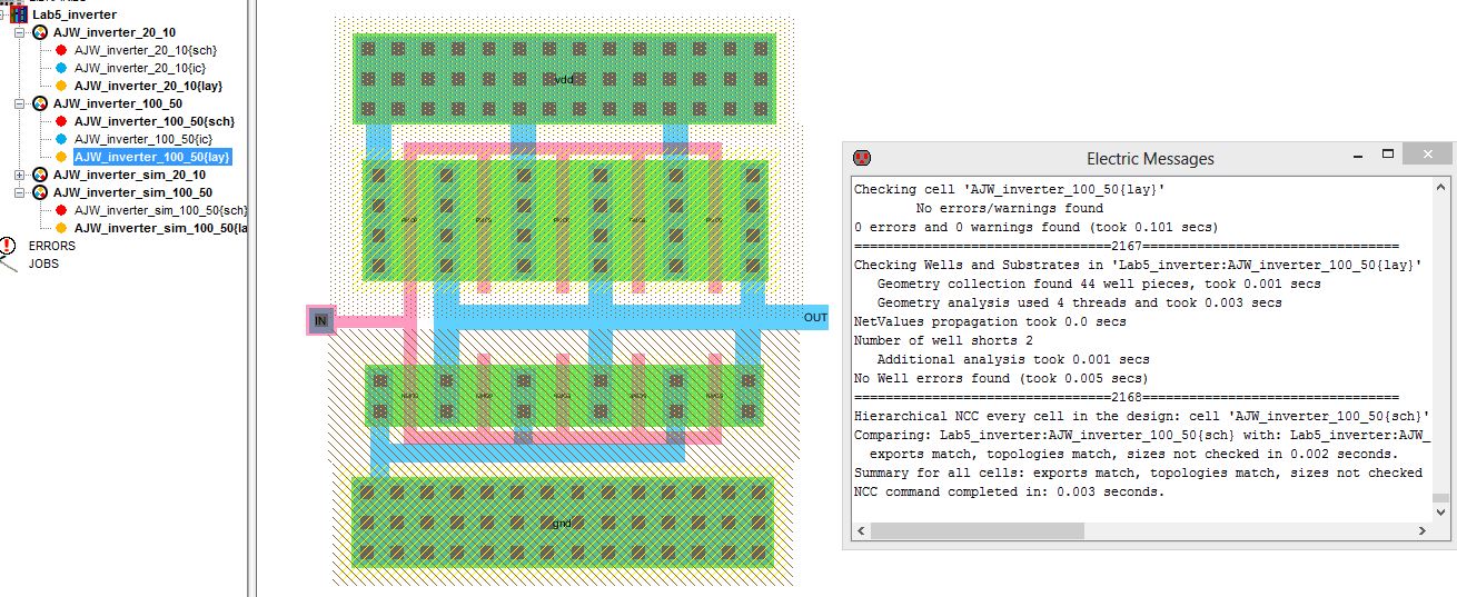
In this design, I want to note the use of the multiplier in order to model a larger sized (M=5 means 5 times the width) Inverter . Note the 4 pins, I exported again. also noticed that all of the design rules are met so that there are no errors in DRC, ERC, and NCC.
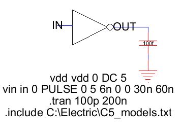
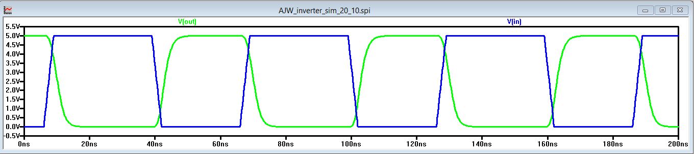
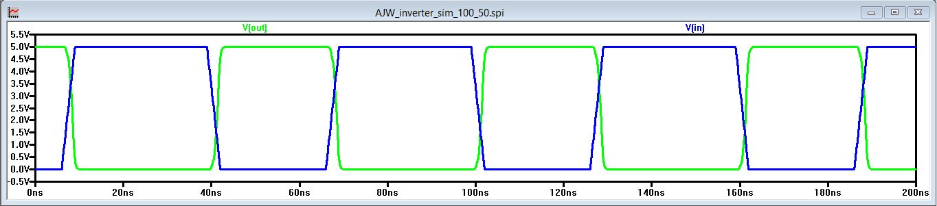
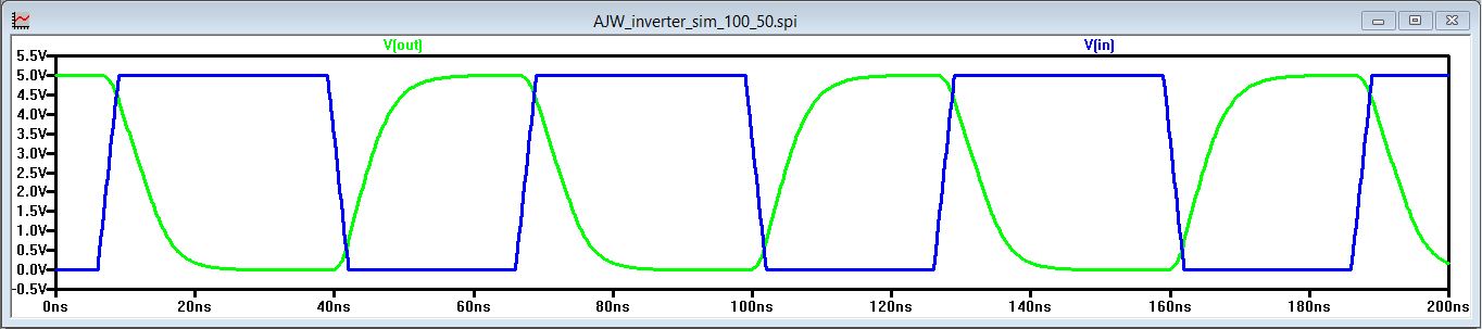
The Spice Simulation for the inverter driving capacitive loads is shown below:

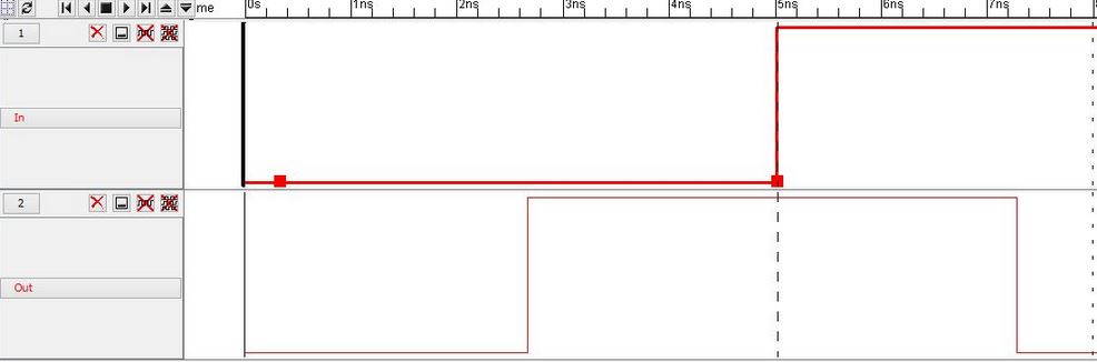
20/10 with a 100fF load:

100/50 with a 100fF load:
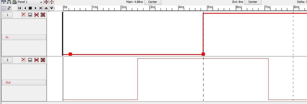
20/10 with a 1pF load:
100/50 with a 1pF load:
20/10 with a 10pF load:

100/50 with a 10pF load:
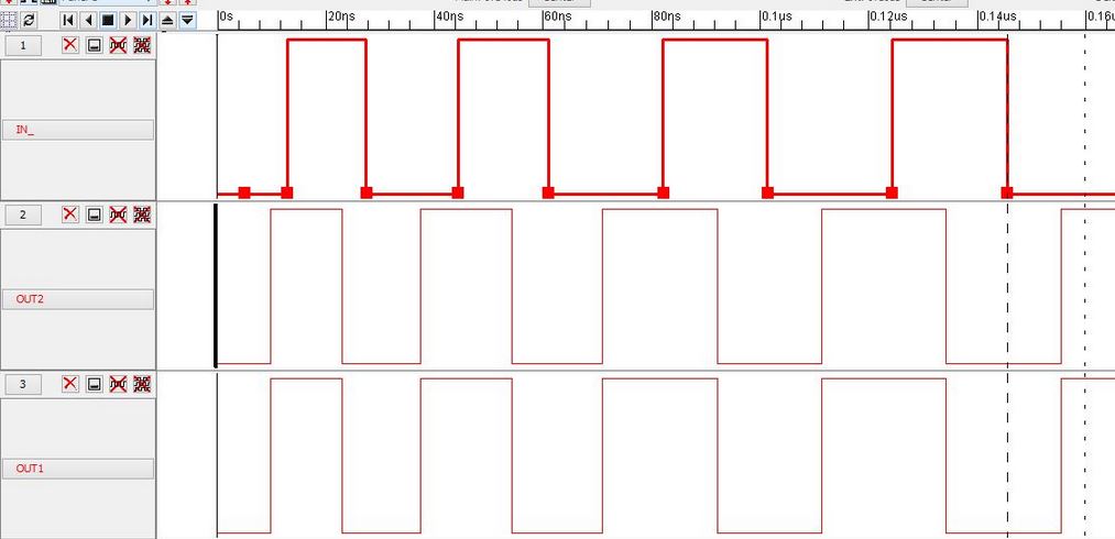
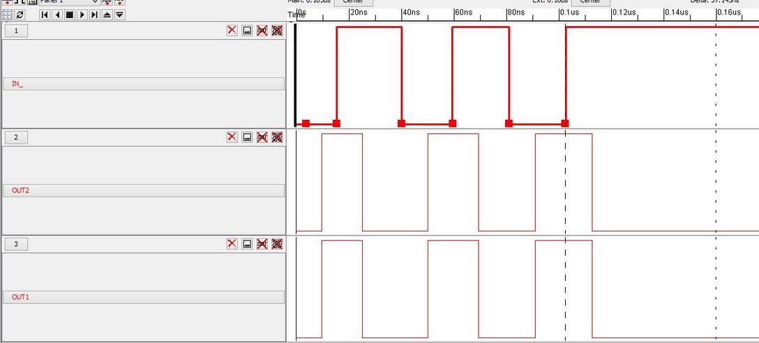
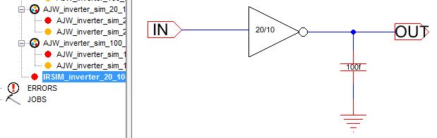
ALS simulations/schematics:
Below is the ALS simulation results when driving 3 seperate capacitance loads.
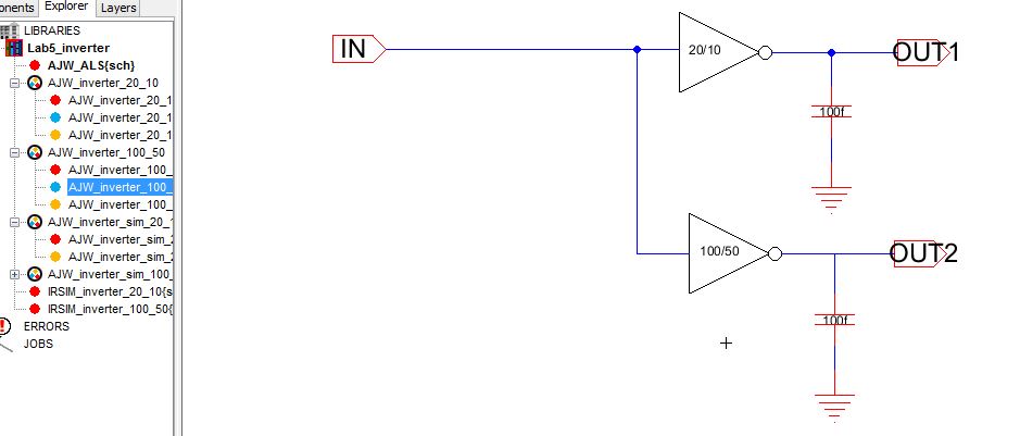
Since the ALS will not take into account the delay of the transistors, but rather a more ideal logic design, we will not see a difference in the output delay between the outputs. below is the 3 capacitor loads:
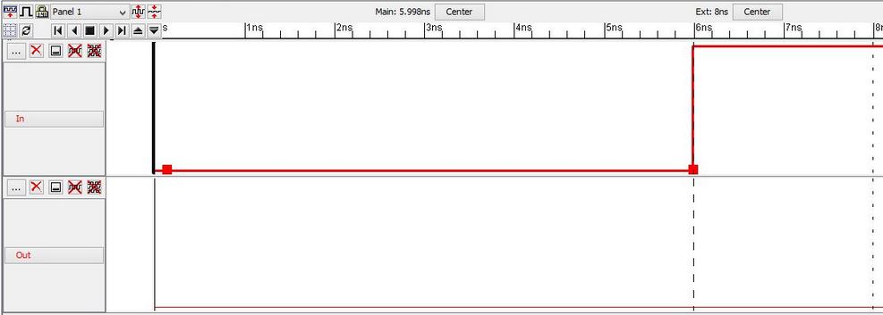
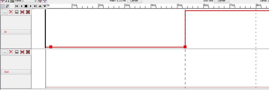
100fF capacitor:
1pF capacitor:
10pF capacitor:
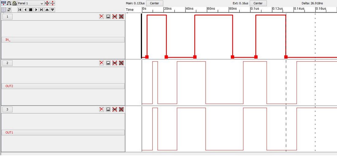
After looking at all the wave forms, we notice that there is no delay which makes sense since we are using the ALS.
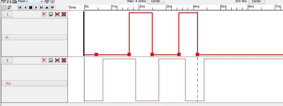
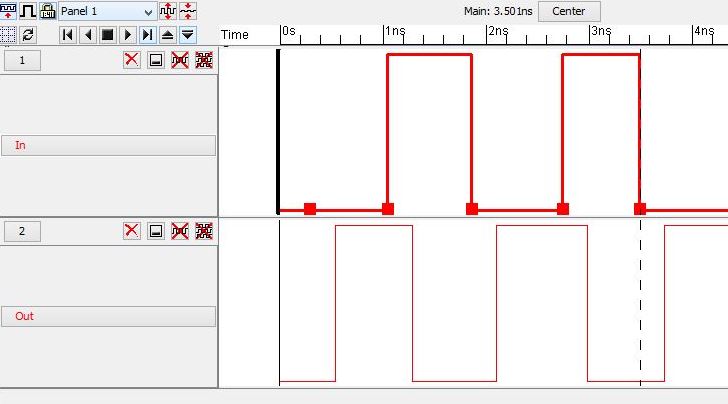
Next is the IRSIM simulation, again, using the three different load capacitors of 100fF, 1pF, and 10pF. Below are the schematics and wave forms:
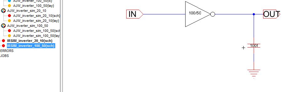
for the 100fF capacitance, we get a delay (20/10 is on the right and 100/50 is on the left):
for the 1pF capacitance:
for the 10pF capacitance:
After looking at the simulations, it is apparent that the IRSIM simulation is a great tool to model at the transistor level due to the delays associated with the load capacitances.
Once done, I saved my work and backed it up.

Return to Adam's Lab Directory by clicking HERE