Lab 4 - EE 421L
IV Characteristics of NMOS and PMOS devices in ON's C5 Process
Authored
by: Adam James Wolverton
Email: Wolvert9@unlv.nevada.edu
Today's
date: 9/27/2013
Lab
description:
In
Lab 4, We use the 3 terminal MOSFET symbols for NMOS and PMOS where the
substrate (body) of the NMOS is connected to "gnd" and the n-well body
of the PMOS is connected to "vdd." We will create the schematics,
layout, and simulation schematics for a 10/2 sized NMOS and a 20/2 PMOS using the C5 process.
Lab Results:
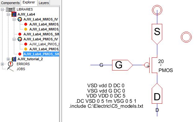
I
created the schematic cells for IV curve characteristics of a 10/2 NMOS
and a 20/2 PMOS, as shown below. I also set the spice model for the
NMOS and PMOS, which are seen in the C5 model file. The way I drafted
these MOSFETs, was through choosing the NMOS and PMOS transistor
nodes in the components tab. Then I queried the components to
change the widths and lengths respectively.Also, I have the DRC, NCC,
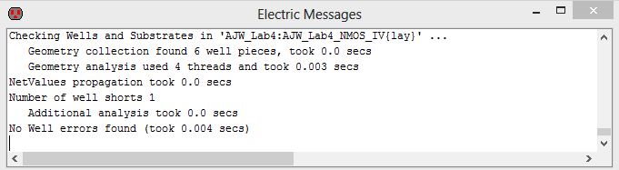
and ERC for the circuit compared to the layout below. 


Here is the layout of the NMOS transistor and the NCC and the ERC
checks out between the schematic and the layout. 
The same goes for the layout of the PMOS transistor, the ERC and the
NCC check out between the Schematic and the Layout. 

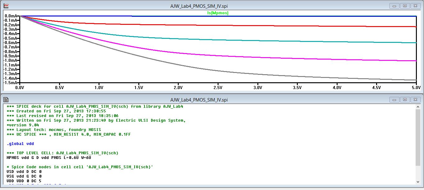
Here are the simulation schematics along with the simulations of the IV curves for the NMOS and PMOS transistors. 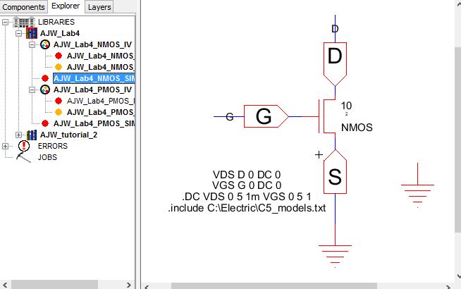

After I finished the simulations and checks I backed up my lab report .
My library used for this lab is located HERE
To return to Adam's other EE 421 Labs click HERE