Lab 3 - EE 421L
Authored
by: Adam James Wolverton
Email: Wolvert9@unlv.nevada.edu
Date: September 20, 2013
Lab Description:
This
lab will be on the layout of the 10-bit DAC I designed and simulated in
Lab experiment 2. It will contain the following:
1) Layout of a 10K resistor using the n-well node.
a) Discussion of how to select the width and length of the resistor by referencing the
process information from MOSIS.
2) Use this n-well resistor in the layout of my DAC.
a) Discussion of how the width and length of the resistor are
measured by Electric.
3)
Ensure that each resistor in the DAC is laid out in parallel having the same x-position but varying y-positions (the
resistors are stacked).
4) Inputs and outputs (exports) should be on metal 1
5) DRC, NCC, and ERC your design (show the results in your lab report)
6)
Place your final jelib in the lab3 directory, with a link on your lab report, so the grader can examine both
the layout and schematic (and simulations)
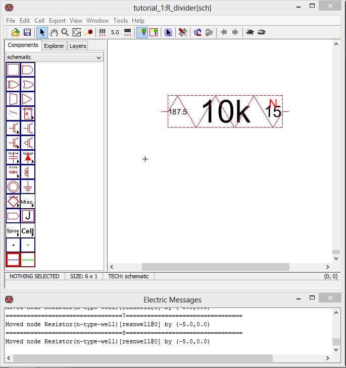
1)
When laying out the 10K resistor using the n-well node we must select
the length and width in accordance to the MOSIS C5 process. After
checking the process, it states that the sheet resistance is 800 Ohms
per square. We determine that suitable dimensions are a length of 187.5
and a width of 15, but the measurements is excluding the region around
the n-well resistors contacts. knowing this, we should decide to sheer
a little bit off and choose a length of 180 since the resistance calc
is such a small portion of the actual n-well. Below is the n-well node
10K resistor:
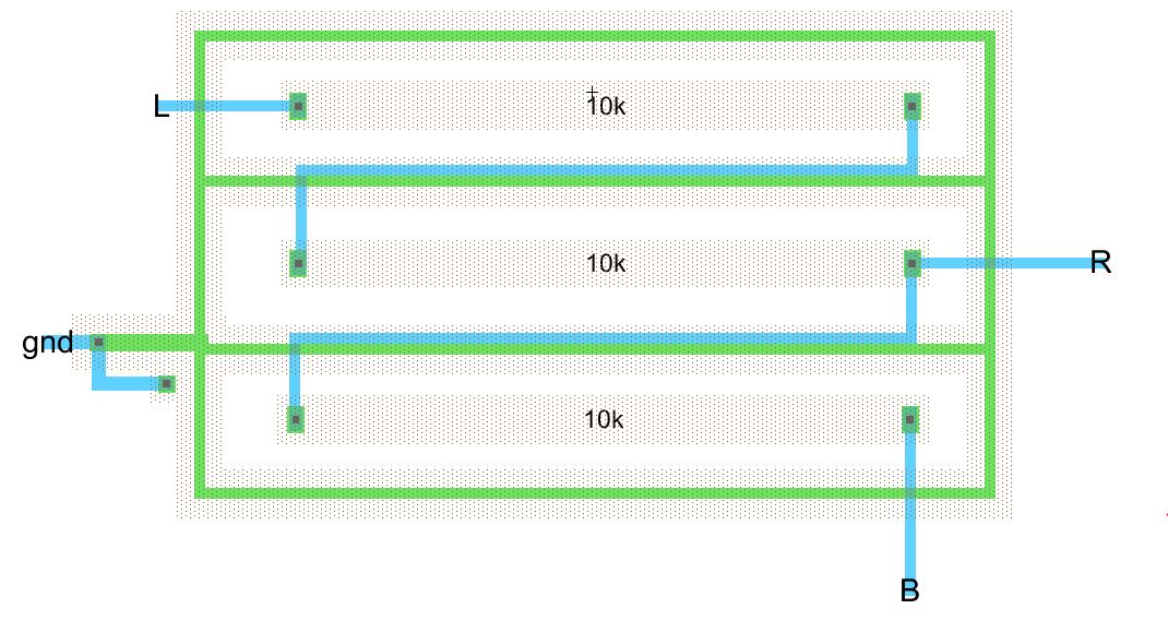
Below shows the schematic for the voltage divider and below that shows the icon and layout I made for the Divider.
Schematic:
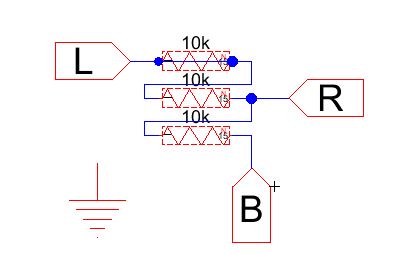
Schematic Icon:
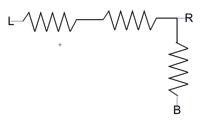
Voltage Divider Layout:
Now,
10 of these are strung together in parallel to create the 10-bit DAC.
the Schematic and layout is provided below for the DAC:
Schematic:

Layout:

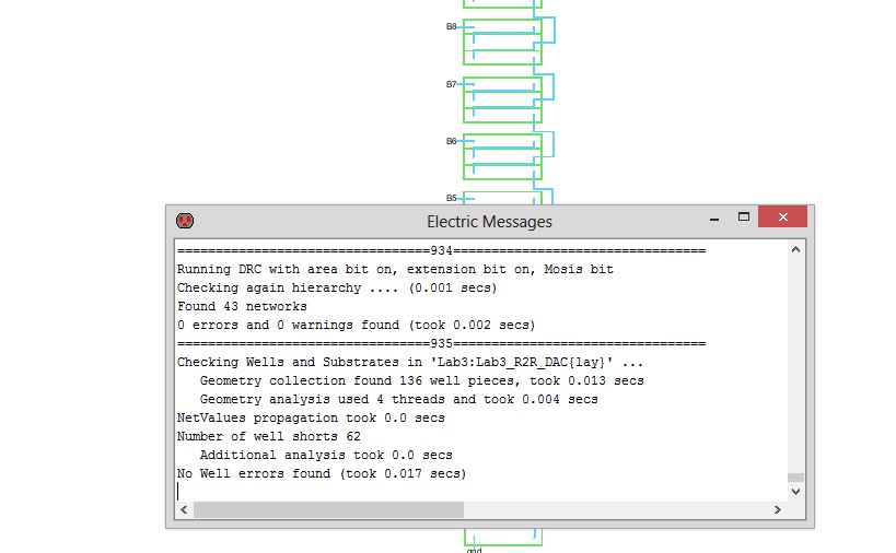
DRC and ERC check out with the layout of the DAC as shown below:
NCC checks out as well for the schematic:

After I finished I backed up my work below:
HERE is a link to my Lab 3 Jelib I used for my lab.
Return to Adam's EE 421L Labs