
Lab 2 - EE 421L
Prelab Work with Narrative:
1) I downloaded the lab2.jelib file and opened the library in Electric, then used Cross-Library Copy to copy the schematic file for the ADC/DAC into the ee421_ecg621.jelib library.
2) Next I saved the course/lab jelib so that it now will contain the copied cells of the ideal 10-bit ADC and DAC.

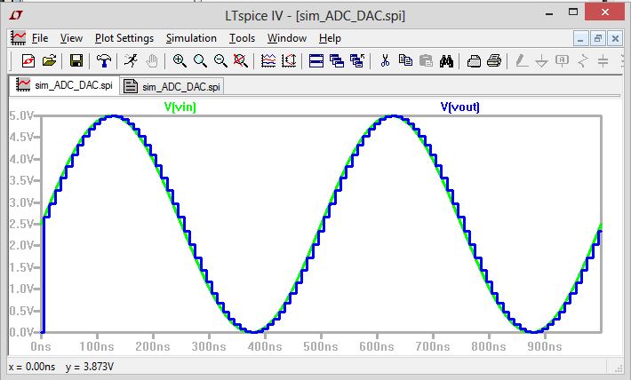
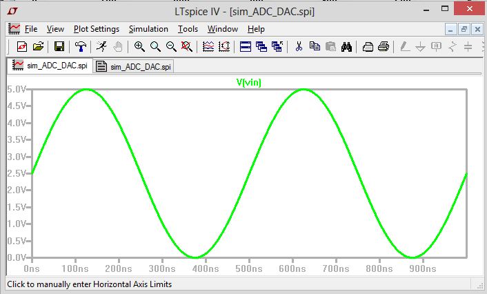
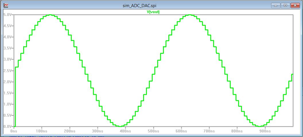
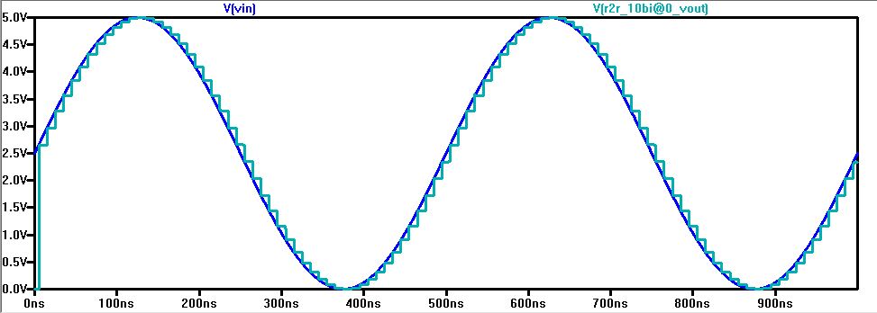
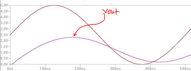
3) After running the simulation, I get the following waveforms for the input and output. B[9:0] refers to a digital encoding for the analog Vin. And Vout reconverts it.
Understanding of ADC and DAC:
The original signal is a "beautiful" sinusoid with a 5 Volt peak to peak as seen below. This is prior to entering the ADC.
The signal is then converted to a digital signal as shown on 10 seperate plot planes below. If # of bits increase, then the quality of resolution increases.

Determining Least Significant Bit
Lab Report:
1) Using the 5-bit (expanded to 10-bits) resistor DAC Topology given in Figure 30.14, I implemented this into my own DAC. as seen below, where the all of the resistor values are 10KOhm. After the resistor schematic was created I placed a copy of my personal IC into the ADC to DAC circuit to test out the output. DRC checked out with out errors.
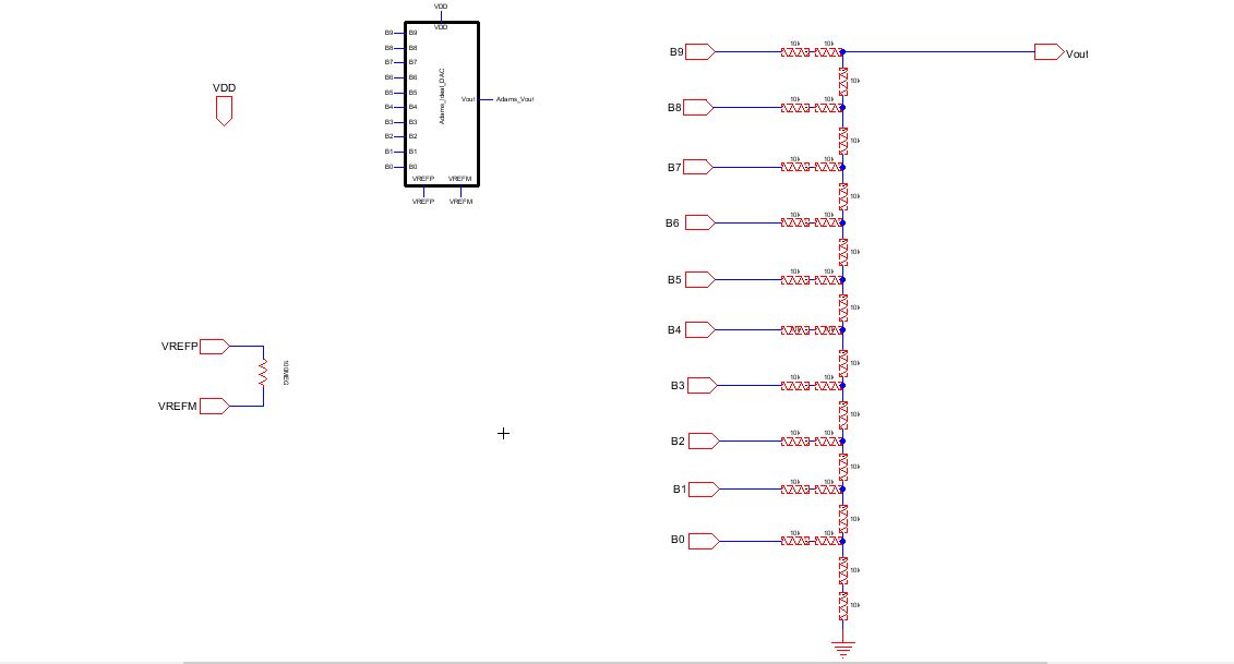
2) How do we determine the output resistance of the DAC? In order to determine the output resistance, one should combine the resistors in parallel and series to reduce to eventually a resistance of R. This is only if all resistors used in this design are the same value.
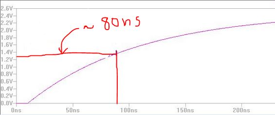
3) Delay, while driving a load: The Time delay we get when driving a 10pF load, is about 100ns, however the simulation results shows that it is more about 80ns.
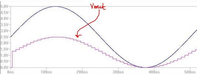
4) The following waveforms show how the DAC reacts with a capacitive load, resistive load, and an RC load in that particular order.
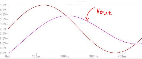
Notice the phase shift and smoothing of the choppy signal due to the capacitive load.
In this waveform, we have the resistive load, which shows the voltage drop, but still seems digitized, but still in phase.
This wave form shows the RC load, which is a voltage drop and smoothed out by the capacitor as well as phase shifted. In conclusion we see that the non ideal DAC does not work well when under any load.
5) When the switches in the DAC are implemented with MOSFETs, we would want the resistance of those MOSFETs to be small compared to the resistor values, because voltage drops and time delay can cause the accuracy/reliability of the DAC to be questionable.