Lab 6 - EE 421L
Edgar Solorio,
solori12@unlv.nevada.edu
10/11/13
Pre-lab Work:
* Finish Tutorial 4 and Electric_video_11
Lab work:
In this lab we will create a 2-input NAND, NOR, AND XOR gates to create a 2 bit Full Adder.
I
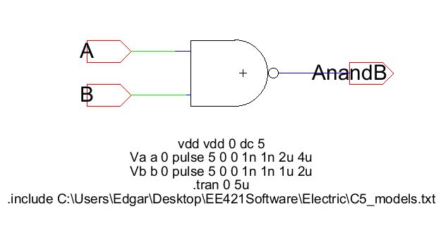
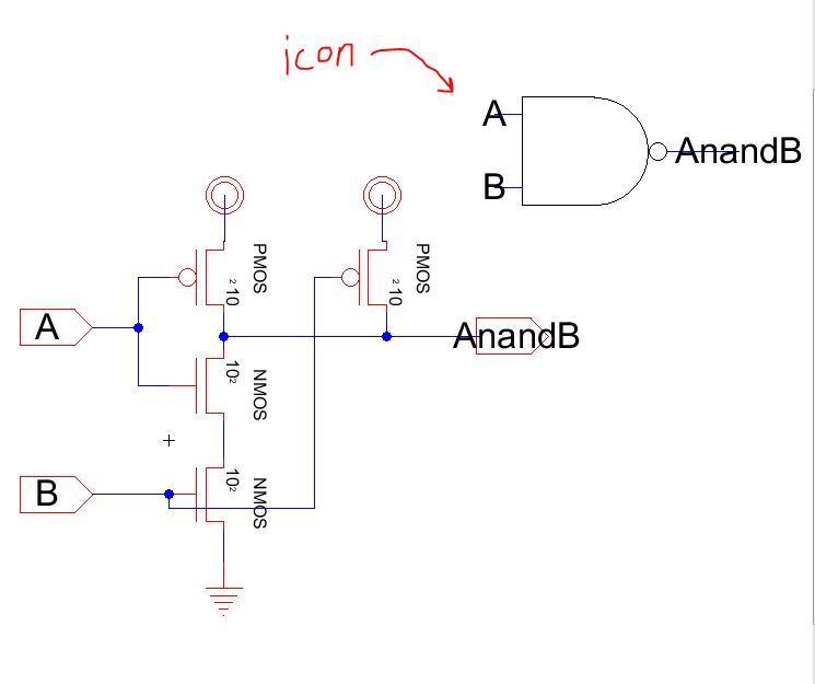
start by drafting the schematic of a 2-input NAND gate as shown in
tutorial 4. The schematic is shown below with my icon model on the top
right of the screen. Note that 10/2 MOSFETS were used (for both NMOS
and PMOS).
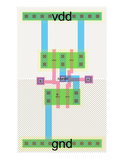
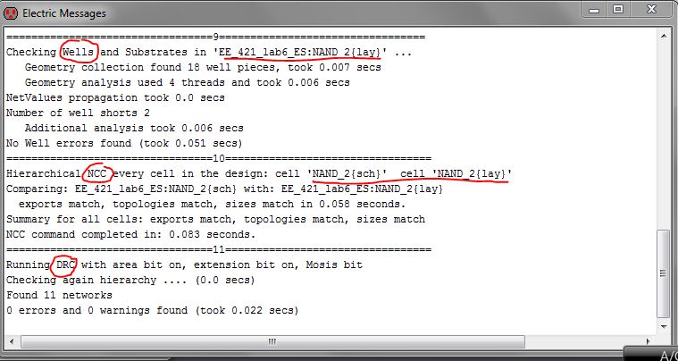
The corresponding layout view for the 2-input NAND gate is shown below along with the DRC, NCC, and well-check results.
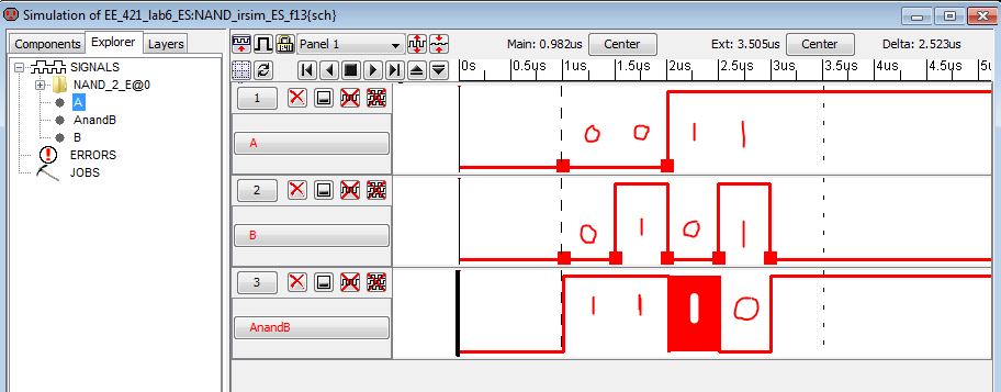
To
test the correctness of both the layout and schematic for the 2-input
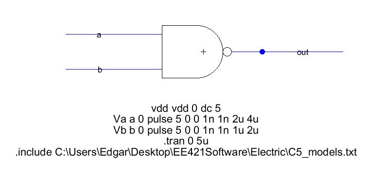
NAND cell, I used LTspice and IRSIM the simulate the logic. Both
simulation results are shown below along with the simulation schematics
used for each.
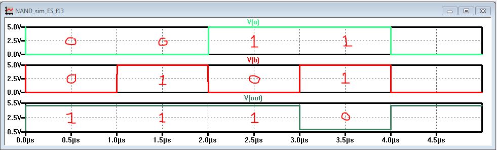
The
simulation results for the 2-input NAND gate for both IRSIM and LTspice
are correct and give the correct truth table values for all 4 possible
inputs.
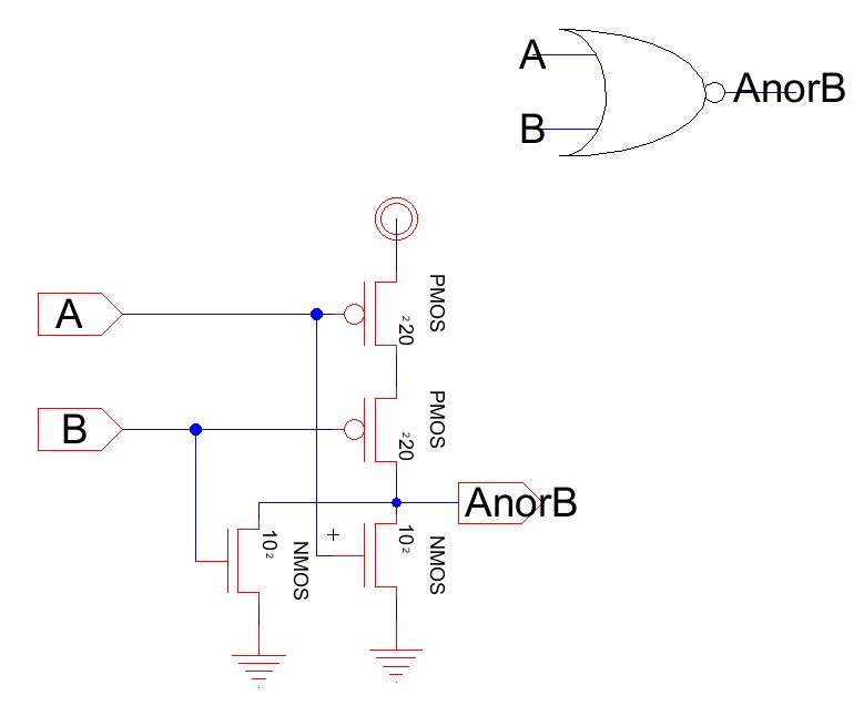
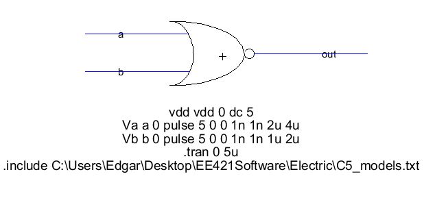
The next step is to create a 2-input NOR gate, but
this time using 20/2 PMOS devices and 10/2 NMOS devices. The schematic
and icon are shown below.
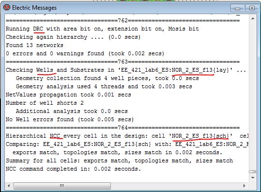
The layout for the 2-input NOR gate is shown below along with the results of the DRC, NCC, and well-checks (showing no errors).
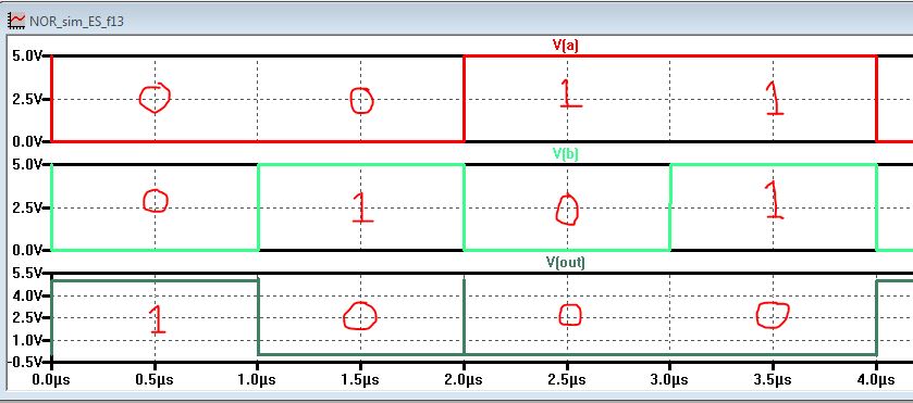
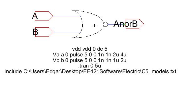
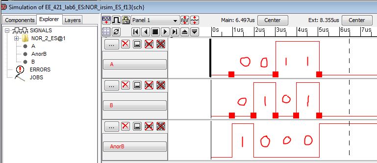
Now
it's time to simulate the 2-input NOR gate using both LTspice and
IRSIM. The schematics used for both simulations are shown below along
with the corresponding simulation result.
The
schematics, layouts, and simulation results for the 2-input NOR gate
are correct, and the right truth table values are shown in both
simulations.
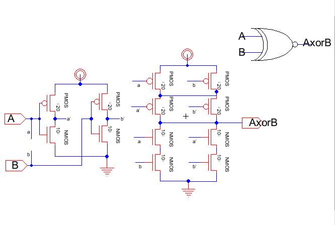
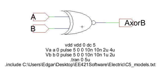
The final gate we will create is the 2-input XOR
gate, which uses 2 inverters and has a total of 12 transistors. The
size of the PMOS will be 20/2 while that of the NMOS is 10/2. The
schematic and icon are shown below for the 2-input XOR gate.
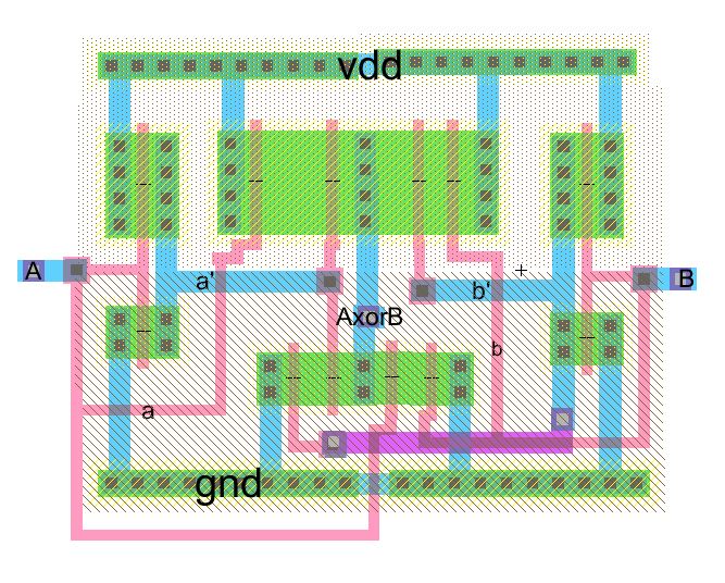
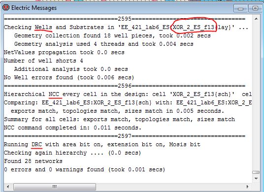
The layout for the 2-input XOR gate is shown below along with the DRC, NCC, and well-check showing no errors.
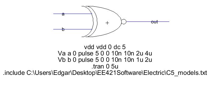
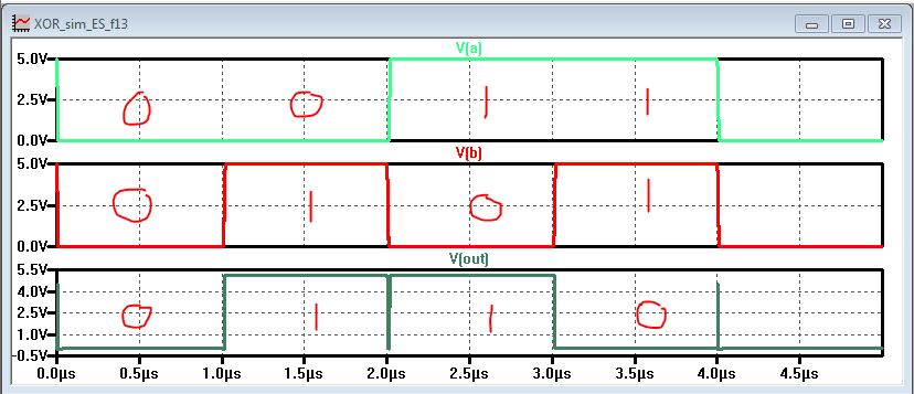
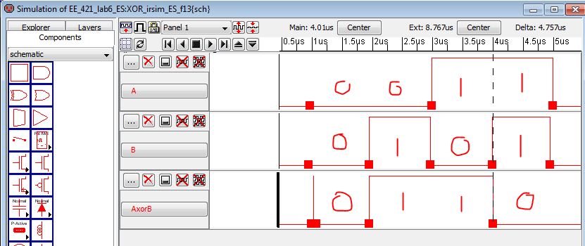
The
schematics used for an IRSIM and LTspice simulation are shown below
along with the corresponding simulation results. Note how the truth
table values are correct for all 4 cases.
I
now create one version of the Full adder using the gates created thus
far and 3 inverters as shown in the schematic below with the
corresponding icon.
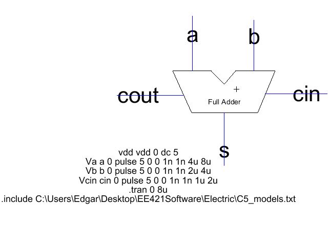
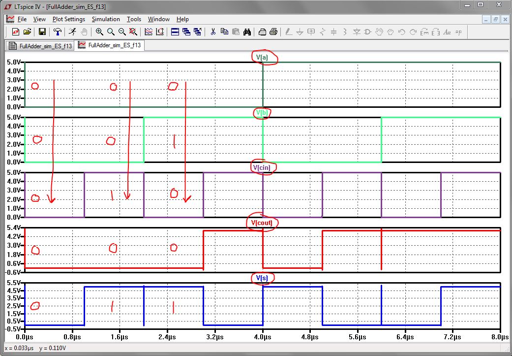
I
simulate this Full Adder circuit using both LTspice and IRSIM, the icon
was used for both as a sim schematic shown below. Although the LTspice
simuation results are corrct, the IRSIM results were a little more
sporadic, and I leave that to human error and my inexperience with
IRSIM.
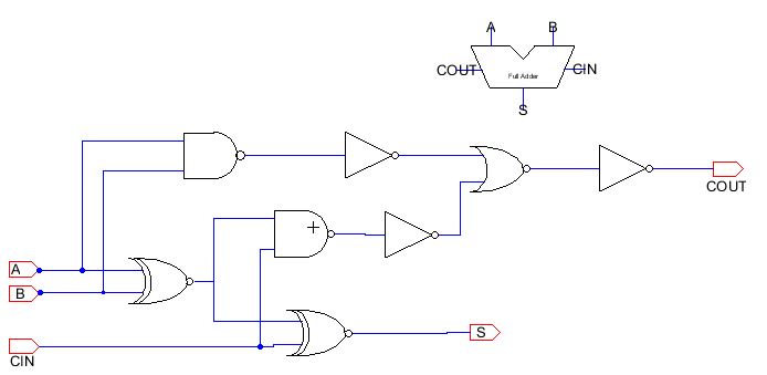
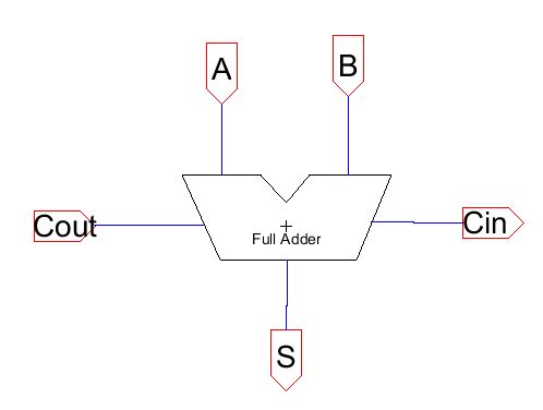
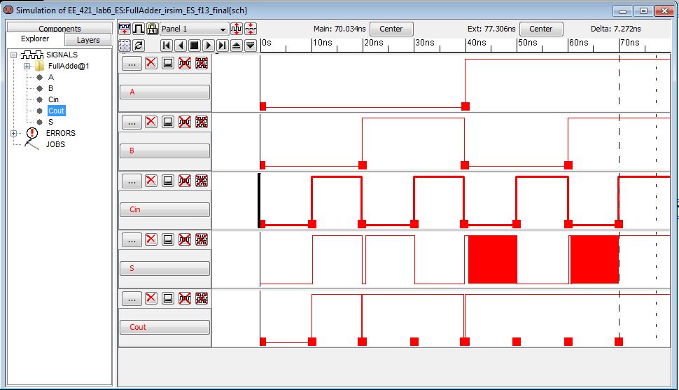
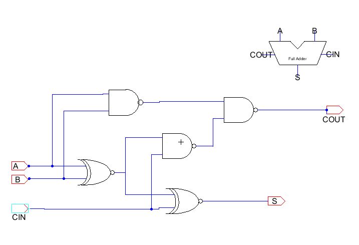
The Full Adder can also be implemented using 3 NAND gates and 2 XOR gates as shown below in the schematic.
since
this Full Adder has the same icon from the previous full adder circuit,
the simulation schematics have been ommited and only the simulation
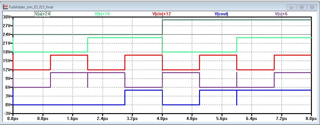
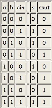
results will be shown below. Note once again that LTspice shows the
correct results for the Truth Table values of a Full Adder (shown
below) while the IRSIM is still beyond my level of expertise to use
correctly.
NOTE:
Do to limited amount of time, I was unable to finish the layout of the
Full Adder, I will work finish that portion of the lab on my own time.
BACKUP YOUR WORK:
As always, back up your work in a safe location as shown below.
A link to my jelib file is found here, lab6
Return to EE 421L Labs