Lab 5 - EE 421L
Edgar Solorio
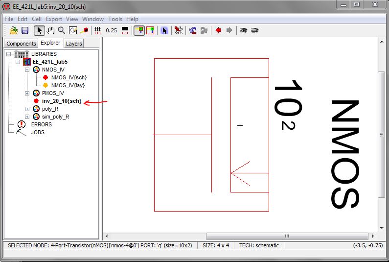
Now create a new cell and name it "inv_20_10", make sure it is a schematic cell, now place the copied content into this cell to get the following.

Repeat the steps above; copy the PMOS device from "PMOS_IV{sch}" and put it into the "inv_20_10 {sch}" cell. Change it's properties to be a pmos transistor.

Since we want a PMOS of width 20, click the device and change it's width to "20". Now turn on the grid by using "Ctrl + G", add a vdd and ground symbol. If the symbols are to large, you can make them smaller by clicking on them and hitting "Ctrl + B", make sure to align them up to grid to avoid "resolution" errors that may occur. The schematic now looks like the one below.

Now add arcs between all the nodes and add export page nodes and export them as shown below to "in" and "out".

We will now create an icon for our schematic which is done by going to View -> Make Icon View.

Click on the new "inv_20_10{ic}" cell from the explorer to reach this window.

Modify the icon so that it looks as shown below.

Go back to the "inv_20_10{sch}" cell and notice that our icon is now complete.

To simulate our inverter schematic, we will now create a new schematic cell named "inverter_sim". Drag and drop the "inv_20_10" icon as shown below and add arcs to the inverter. label the arcs as "in" and "out" and also add the following spice code as shown.

Simulate the schematic and the following results should occur when plotting Vout and Vin. Notice how Vout stays "HIGH" as Vin goes from 0 to about 2.3 volts. Vout then experiences as sharp drop and stays "LOW" as Vin goes from 2.6 volts to 5 volts. This is how an inverter acts,i.e. when Vin is LOW, Vout is HIGH and vice versa.

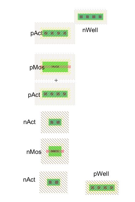
Now that we have the schematic done, we will create the layout of the 20/10 inverter. Create a new layout cell and name it "inv_20_10". Place the following parts as shown below into the cell (note that annotation text has been added to make it clear which nodes are which).

Add the PSPICE model to the pMos device by clicking on it and going to Tools -> Simulation (SPICE) -> Set Spice Models.. and name it "PMOS", if you cannot see the text then change the size to 4 as shown below. Change the size of the pMos node to have a width of 20 as well.

Now click on the nMos node and set it's spice model to "NMOS" and change it's width to 10.

Change the sizes of the pAct, nWell, and pWell nodes to have a width of 20, and change the size of the nAct to have a width of 10 as shown below.
At this point, add arcs from the pMos node up to the pAct nodes, add arcs from the nMos node up to the nAct nodes as well.

Move the Active nodes in close to the nMos and pMos nodes as shown below. Do a quick DRC for errors, most likely the contacts are to close, so seperate them outwards more.

At this point, the annotation text has been deleted, rotate the pMos and nMos by using "ctrl + J" so that they are lined up as shown below, with the PMOS ontop and NMOS on bottom. Do a quick DRC test to see if there are any errors.

Place a contact and metal1 pin as shown below. Create arcs as shown below as well (the gates are connected together, the contacts are tied up to the vdd and gnd contacts, etc.).


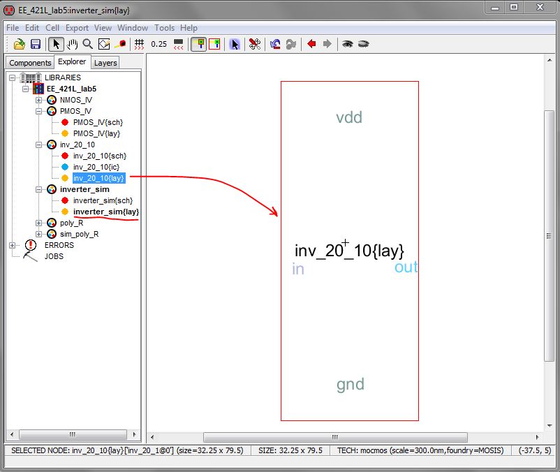
Make sure to save your work if not done so thus far. We will now test our layout by creating a new layout cell named "inverter_sim". Drag the layout from "inv_20_10{lay}" cell as shown below.
Add metal1 arcs, make sure to export the pins for vdd and gnd (which are shown are larger text in the image below). Name the other two arcs "in" and "out" and also add the following spice code as shown below.

Now simulate the layout cell and you get the following results which are very similar to the simulation results when done using only schematic symbols.

Run a quick Well check, NCC check, and DRC check. For some reason, I always get an error in my well check saying that there are 2 shorts but it does not seem to effect the simulation results or design overall.

Now that we have created a layout, schematic, and simulated the 20/10 inverter, we will now do the 100/50 inverter.
To create the schematic cell for the inverter, go into the "inv_20_10" schematic and copy the following material shown below.

Create a new schematic cell and name it "inv_100_50" and paste the material copied from the last step.

Export the pins as "In" and "Out" as shown below. Add multipliers to both the PMOS and NMOS device by clicking on each of them and going to Tools -> Simulation (SPICE) -> Set Multiplier. Change each Multiplier to 5 so that it shows "M = 5". The multiplier is a way to show that there are "M" mosfets in parrellel of the size given by the mosfet, for example, the PMOS of size (width = 20, length = 2) has M = 5 which says there will be 5 mosfets of those size layed out in parrallel. Mosfets layed out in parrallel behave as the sum of there width, therefore; the PMOS is actually a 100 width device (5 * 20). This goes the same for the NMOS to create the 50 width size (5 *10).

Create
an icon by following the process from before and design it to look like
the one shown below. The "100/50" is just text that was added into the
icon cell.

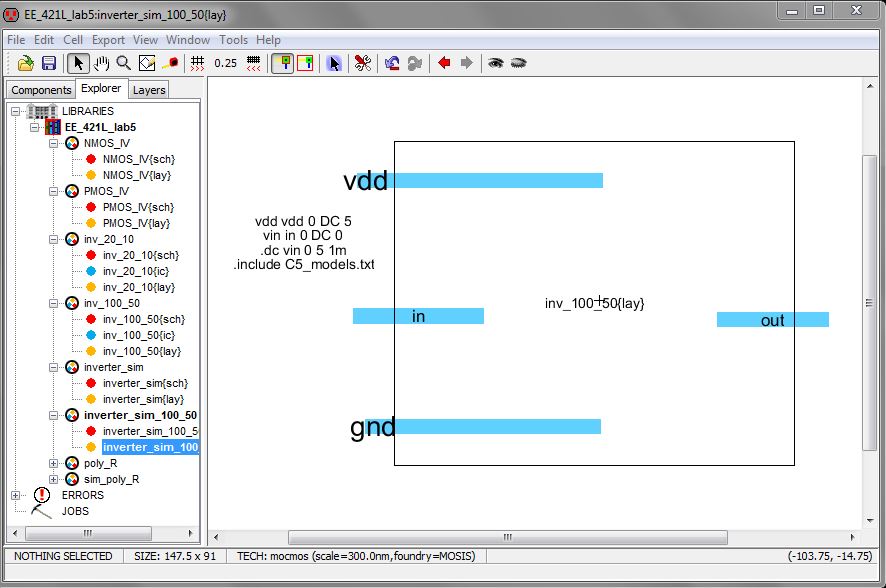
To test out our schematic cell for our 100/50 inverter, create a new schematic cell and name it "inverter_sim_100_50". Drag the "inv_100_50" icon into the newly created cell and add arcs (rename them to "in" and "out") and also add the spice code shown below.

Simulate the cell and you get the similar results as shown from the 20/10 inverter.

Now we need to lay out the 100/50 inverter, first go into the "inv_20_10" layout cell and copy the material as shown below.

Create a new layout cell and name it "inv_100_50" and paste the material pasted from the previous step.

Delete all the metal1 and polysilicon arcs so that you get the leftover layout design.

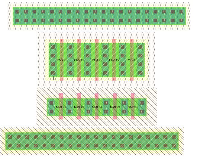
Change the size of the pWell and nWell (top and bottom nodes to be 100 long and 10 wide). Copy and paste the PMOS and NMOS 5 times to have them in parrallel as shown below.

In order to create the 100/50 inverter, we need to put 5 PMOS's and 5 NMOS's in parrallel as discussed previously when talking about spice multipliers (M = 5). Delete the pAct and nAct nodes (the locations are marked with red X's where removed from).

Now connect the top 5 PMOS devices and the 5 bottom NMOS devices as shown below.

The next step is to move the mosfets closer, DRC the layout to check if there are any errors (most likely with the amount of spacing between the Active and mos device.


Create arcs from the sources and drains of the mosfets as shown below.

Last step is to export the following pins as shown below, if you cannot see the text, change it to point size of 8.

Time to check out our current progress, run a DRC check, an NCC check, and a well check.
The results show that the layout and schematic are correct.

We need to test our layout so we will create a new layout cell and name it "inverter_sim_100_50", drag and drop the "inv_100_50" onto our new cell as shown below.


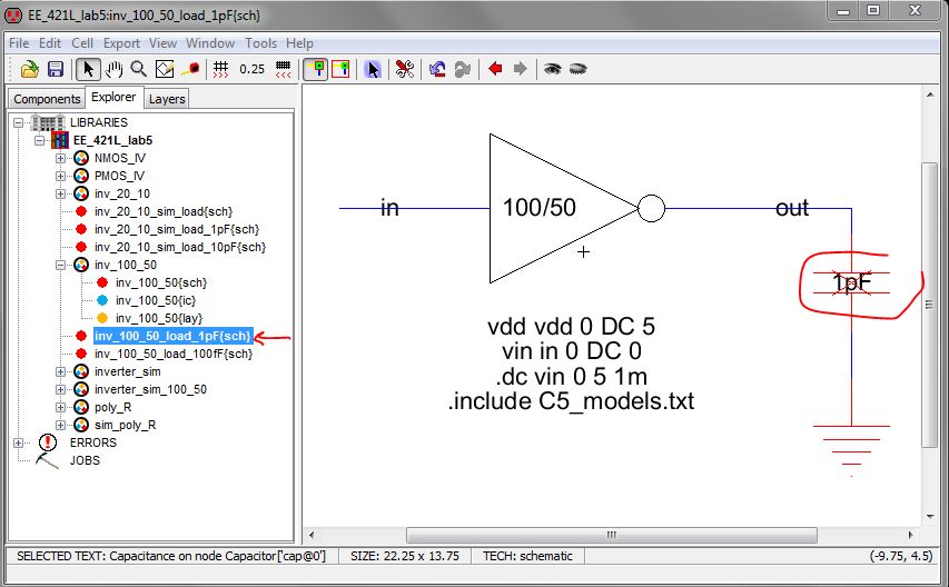
Testing the 20/10 inverter with capacitive loads -


The Spice simulation results are all shown below, the top is for the 100fF load, middle is for 1pF load, and last image is of the 10pF load. Notice that the output does not change when driving different loads!


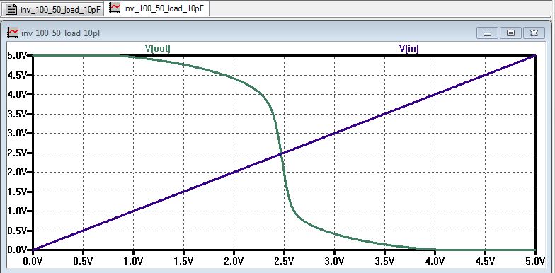
Testing the 100/50 inverter with capacitive loads -
We will follow the same procedure as above to create 3 new cells with each driving either a 100fF, 1pF, or 10pF load on a 100/50 inverter. The schematics are shown below in this order 100fF, 1pF, and 10pF.


The results are shown below for the 100fF, 1pF, and 10pF loads; respectively. Notice once again that the results are exactly the same for all three cases of different capacitive loads.