
Lab 4 - EE 421L
Edgar Solorio
Switch over to the components tab and add an nMos schematic symbol as shown below.

Change the properties of the nMos to have a length of 10 and width of 2, rearrange the values to be on the side of the mosfet as shown below.
Add
a Pspice Model to the nMos by clicking on the nMos and then go to Tools
-> Simulation(spice) -> Set Spice Model. Change the spice model
to
"NMOS" as shown below.

Now add off-page nodes to the schematic and wire them up to the nMos device and export them as shown below, G for gate, D for drain, and S for Source.
Add
a ground symbol to the side of the schematic for future use, this will
be where the layout nMos p-substrate will ground to. Your schematic
should look like the image below so far, if the ground symbol is to
large, you can change it's size by clicking on it and typing "ctrl+b".

Our
nMos schematic is now nearly complete, we will now switch to creating a
pMos schematic. Create a new cell and name it "PMOS_IV_XX" where the XX
are your initials. Add a new pMos component to the schematic cell as
shown below.

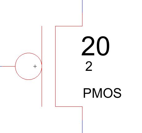
We
will change the length, width, and add a spice model like how we did
for the nMos device. Change the length to 20, width to 2, and add a
spice model named "PMOS". Move the values around to have a similiar
view as shown below.
Now add some off-page nodes and connect them to the pMos device, also add a vdd symbol which will be used for the layout schematic to connect the body of the pMos to vdd.
Export the off-page nodes as shown below.

If we do a quick DRC of our two schematic cells for nMos and pMos, we see that we have no errors thus far.

Now we will create the layouts for the nMos and pMos schematic cells, we will start off by creating a new layout cell and naming it "NMOS_IV_XX" where XX are your initials as seen below.
Notice that creating this layout has now grouped your schematic cell and layout together into one group.

Start
off by switching to the components tab and adding 2 "nAct", 1 "nMos",
and 1 "pWell" as shown below. Annotation text has been added to make it
clear which parts are which.

Change the size of all the parts to have a length of 10 and width of 5 as shown below.

Now create an arc from the nMos part up to the nAct parts for both nAct's as shown below.

Move
the nAct's close to the nMos device and place the pWell near the bottom
of the entire assembly as shown below. Make sure to overlap the two so
the wells connect. If we do a quick well check we see that we get one
error that states the substrate is not connected to ground, we will fix
this error later but for now let it be.

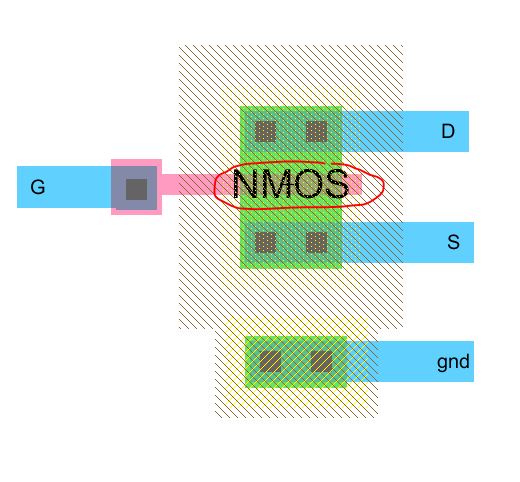
The annotation text will now be removed, click on the nMos device and add a pspice model, do this by going to Tools -> Simulation (spice) -> Set Spice Model and naming it "NMOS". If you cannot see the "NMOS" label, change the size of the text to 4, Also add a contact (poly to metal1) to the left of the nMos device.

Connect
the poly from the Nmos device up to the contact and connect metal1
across the nAct, contact, and pWell nodes. Export these metal1 pins as
shown below. Make sure for the pWell, you export it to "gnd", it must
be lowercase to match the symbol we placed in the schematic cell.
If you haven't saved your work yet, do so now. We will now move onto creating the PMOS layout by creating a new layout cell and naming it "PMOS_IV_XX" where XX are your initials as shown below.

The
process for creating a pMos will be very similar to how we created the
nMos layout. Place the following parts onto the editor, annotation text
has been added to make the parts clearer to see.

Change
the size of the pAct's and pMos to length 20 and width 5, but change
the nWell size to length 10 and width 5 as shown below.

Create arcs from the pMos node up to the pAct nodes as shown below.
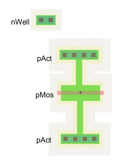
Move
the pAct nodes close into the pMos node as shown below and move the
nWell so the pwell of the node overlaps the pwell of the pAct as shown
below. Do a quick well check, if you have errors, it is most likely
either the arcs are overlapping or your placed the pAct's to close to
the pMos node.

The
annotation text has now been deleted, click on the pmos node and add a
spice model by going to Tools -> Simulation (spice) -> Set Spice
Model to "PMOS" as shown below. Also add a contact (poly1 to metal1) to
the left of the pMos node as shown below.

Create arcs from the poly of the pMos to the contact as well as metal1 arcs as shown below. Export the metal1 pins as shown below. Notice that the nWell is exported as "vdd" all in lowercase to match the vdd symbol in our schematic cell.

Here is a quick 3D view of the pMos device we created so far.

Now that we have finished the NMOS and PMOS schematics and layouts, it is time to save our progress if you have not yet. To simulate our devices, we will create a new cell named "sim_NMOS_IV_XX" where XX are your initials to simulate our NMOS device. Drag and drop the "NMOS_IV_XX" schematic onto the new cell we just created. If you cannot see the component and exports, click on the box and hit the eye arrow as shown below.This view looks very strange and so we will create an icon to have a better representation.


You
can edit the "resistor like" component by clicking on it and hitting
"Y" to edit the lines. Move the pin labels and create the icon to look
similar to the one below.

Now go back to the "sim_MOS_IV_XX" schematic and drag and drop the newly created icon into the cell. Notice that it looks cleaner and nicer then when we previously just dragged and dropped the "NMOS_IV_XX" schematic which had off page nodes.

We will now create an icon view for our pMOS device and save ourselves trouble, go into the "NMOS_IV_XX" icon cell and select the entire device as shown below and copy it.

Now
lets go into our "PMOS_IV_XX" schematic cell and create a new icon,
enter that icon as shown below and delete the box and label. Paste the
contents from when we copied in the previous step and you should have
the same thing as shown below.

Delete the blue-green orbs and place the S,G,D as shown below, add a circle component into the icon view and change it's size to x = 1 and y =1 so you can have the same view as below.

Now go back into the "sim_NMOS_IV_XX" schematic cell and add spice code as shown below.

Simulate the schematic and plot I(Vds} to get the IV characteristic curves shown below for the NMOS device.

Go into the "sim_PMOS_IV_XX" schematic cell and add spice code here as well as shown below, be careful, the code might look similar to the previous one for the NMOS but voltages are defined differently, i.e, VGS and VSG are connected in opposite polarities in the spice code.

Simulate the schematic and plot I(Vsd) to get the IV curve characteristics of the PMOS device shown below.

Finally, save all your work and create a backup file for your lab4 report.
Here is the link to my jelib for reference lab4_jelib
