Lab 3 - EE 421L
Edgar Solorio
solori12@unlv.nevada.edu
9-13-2013
Lab Work-
1.) We
want to create a 10-bit DAC layout as designed in the Lab 2 schematic.
We will open up electric and create a new node called "R_2R" as a
SCHEMATIC CELL. Go to components and add an N-well resistor, DO NOT USE
A NORMAL RESISTOR. To change the length and width of the Resistor, we
will click it and change it's properties as shown below. The width has
to be a minimum of 12 lambdas as described by the C5 CMOS process which
can be found at C5 CMOS process design rules Here is a quick glimpse of the design rules for an N-well width and spacing.
For
our 10k resistor, we will use a width of 15 and follow the equation
R_total = R_square *(L/W). Solving for Length, we get L =
(R_total/(R_square)*W. The R_square is approximately 800 ohms/square as
shown below and found at this link https://www.mosis.com/cgi-bin/cgiwrap/umosis/swp/params/ami-c5/t99j-params.txt
With these numbers, we calculate the length as L = (10k/.8k)*15, L = 187.5 lambdas.

Now we will use the 10K N-well resistor for our layout of our DAC, create
the same layout as before, we shall start by having our basis as shown
below. Add off-page nodes and Export them with Ctrl+E to have the same
names as below.

Now go to View -> Make Icon View to create an icon for our subcircuit which will be used for our DAC design.
Now
go into the icon cell for the R_2R and change the design and pin
layouts to resemble the icon design as shown below. You can use the
Components to add artwork and edit them by clicking on the artwork and
hitting "Y".
Now
we will create a new cell for the 10bit DAC using our new icon to make
the design more simple. Name this new schematic cell
"10bit_DAC_with_icon".
and drag the R_2R icon into the new schematic
cell. Create the design to be similar to this and export the off-pages
like before.
The
schematic for our new DAC circuit using icons is done for now, we shall
move forward to the layout of this circuit. Create a new Cell and call
it "10bit_DAC_with_icon" and save it as a layout cell as shown below.
We
will begin by adding three N-well resistors onto the new layout, change
their length to 187.5 and width to 15 and stack them up vertically so
they all have the same x-position but varying y-positions as shown
below.
Notice
from the image below that the length and width of the N-well resistor
are measured from top to bottom edges for width and length is measured
from the edges of where the contacts are. This is because the
resistance of the contacts is negligible and are therefore not
incorporated in the actual length of the resistor.
Make
sure the spacing between the resistors is correct, minimum of 18
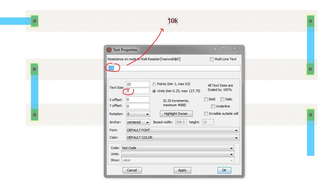
lambdas, hit F5 to run the DRC to make sure. Ctrl+I the resistors and
change their Well Resistance to 10K and increase the size of the text
to 5 scale units. Add some metal to connect the three n well resistors
in series as shown below, change the metal size to 5 as well. DRC the
layout so far.
Follow
the pattern as shown below until you have ten "R_2R" sub layouts. Make
sure to export the pins on the left side where "vin" is labeled as the
appropriate label from either B9 to B0. The top most 3 resistors has a
"vout" where our DAC result will come from. Make sure to DRC when
complete to make sure there's no errors in spacing, metal widths, or
resistor dimensions.
Your
10bit_DAC_with_icon layout top of the circuit should now look similar
to the figure below after exporting the nodes as shown, change their
size to 8 if you cannot see them at first.
Running a DRC, Well Check, and NCC shows that there are no errors within either schematic or layout and they both match as well.
Now
let's go back to our "10bit_DAC_with_icons" schematic and create an
icon for it. Simply do View -> Make Icon View and an icon as circled
below should appear.
Edit
the icon as discussed before in Lab 2, simply click on the icon cell
and rotate/move the pins, resize the box, etc. until you get an icon
similar to the one below.
Notice how the inputs were ordered from B0
to B9 in the original icon made, make sure to move them around to get
them to go from B9 to B0 as shown below.
To
see if our new "icon" of a voltage divider composed of 2 resistors in
series to form 2R and another resistor to form R, we will open up
"sim_ADC_DAC{sch}" and create a duplicate cell and call it
"sim3_ADC_DAC{sch}". Enter the new sim3 cell and delete the items
circled below.
Now place the new "10bit_DAC_with_icon{ic}" icon onto the "sim3_ADC_DAC{sch}" and connect it as shown below.
Once
we run the simulation results with the spice code as shown above, we
get the following results, which is the same exact output fromm
"sim_ADC_DAC" which uses an ideal DAC, as well as being the same output
from "sim2_ADC_DAC" which uses a DAC created out of resistors.
The
Jelib file containing all of this lab's work on the iconization of the
resistor ladder DAC as well as simulation settings can be found here. Simply right click on the link and save the target onto your desktop and open it with Electric.
BACKING UP THE WORK, here I show that my lab3 is safely backed up in my drop box account along with the other two labs.

Return to EE 421L Labs