Lab 2 - EE 421L
Edgar Solorio
solori12@unlv.nevada.edu
9/6/2013
Prelab Section -
1.) After
launching Electric, open up the lab/course jelib (in this case
ee421_ecg621.jelib) and the lab2.jelib. Copy sim_ADC_DAC{sch} with all
its subcells and related views by following the inputs in the window
below. When finished, hit "Done" and close the lab2.jelib library so
only the course/lab jelib is open.

Now
save your course/lab jelib by clicking on the floppy disk button as
shown below. Run the simulation setup in the sim_ADC_DAC as seen below.

After running the simulation, you should get the following results after plotting Vin and Vout.
2.)
The ADC unit converts an analog signal into a digital signal, this unit
is designed to sample and hold the value at a discrete point in time of
the sine wave specified by the spice code in sim_ADC_DAC{sch}. The
results above shows a staircase shaped Vout signal although Vout should
be an analog signal since it comes out of the DAC unit. Since the clock
pulse that is provided to the ADC and DAC unit has a period of 5ns,
there is a finite amount of time needed for sampling and holding the
input values, and that manifests asthe staircase shape seen above in the simulation results.
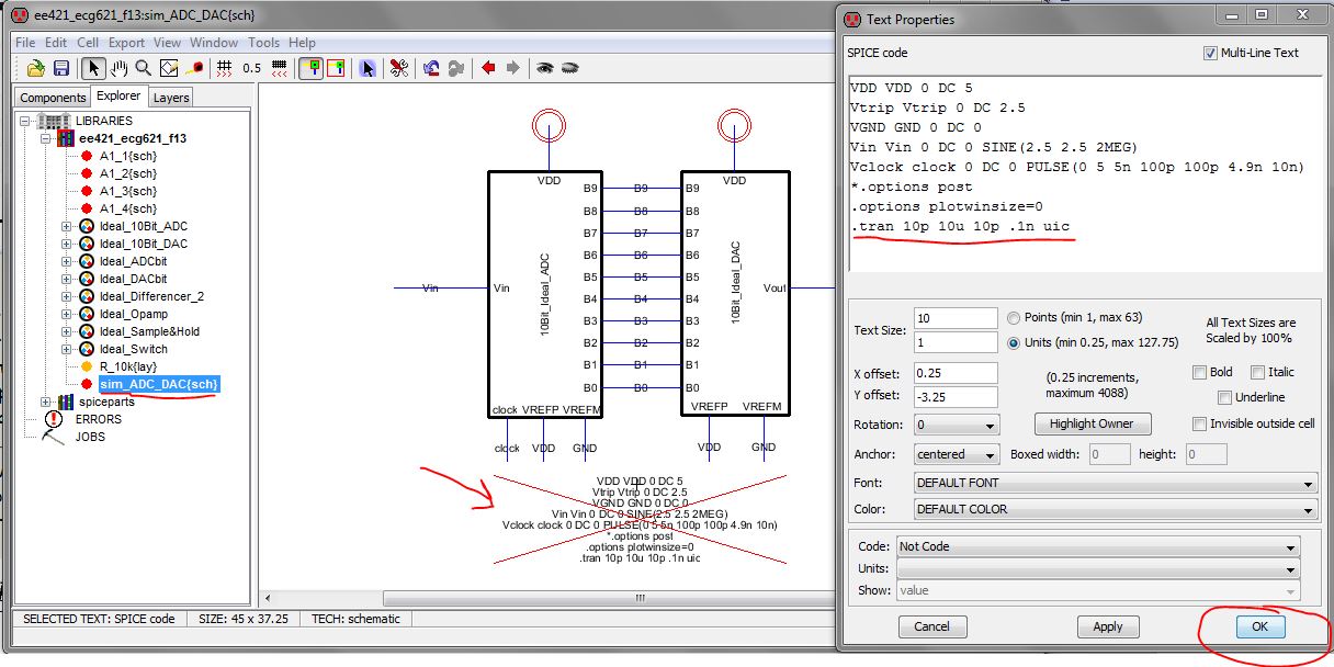
Now
change the spice code on the sim_ADC_{sch} cell by clicking on it and
then ctrl+i to open up the properties box. Change the .tran line to
".tran 10p 10u 10p .1n uic" as seen below.
The
simulation results should look as the results shown below. By changing
how long the transient ran for, we can "zoom out" and see Vout
resembles Vin better.
3.)
Since the ADC is a 10 bit unit, it recognizes 2^10 (= 1024, 0 to 1023)
discrete values that are outputted as a digital code on B[9:0]. That
means the minimum voltage change on the ADC's input to see a change in
the digital code on B[9:0] is given by delta_V_min = (V_high -
V_low)/(2^n). Where V_high and V_low are used as reference levels for
the ADC. Notice that as the difference between V_high - V_low gets
larger, we get a bigger range for the ADC to accept, but our resolution
gets worse since the minimum voltage change to see a change at B[9:0]
gets larger.
In
this example, our V_high = 5 volts, V_low = 0 volts, and 2^10 = 1024,
therefor delta_V_min = 4.88mV. In order to determine which bit is the
least significant bit (LSB) we will create a ramp signal to clearly see
the outputs from B[9:0]. To do this, we will change our input sine wave
into a pulse wave with a 500nS rise time, follow the settings as shown
below.

Run
the simulation and you should be able to see all of the outputs B9:0,
as well as the input (as a ramp), I have shown only Vin, B0, and B1 to
keep it simple. Notice how B1 changes at half the speed of B0, this
pattern continues all the way upto B9. This indicates that B9 only
changes with major fluctuations in the input Analog signal, i.e. it is
the most significant bit. Our LSB is the one that changes the most to
our input signal, which happens to be B0 in this case as shown below.
Postlab Section -
1.) The design of a 10-bit DAC using an N-well R of 10k -
We want to design a simple 10-bit DAC using N-well resistors of 10k each as shown in the following figure.
We
first start by creating a new schematic cell (Cell -> New Cell) and
naming it something useful such as "R2R_10bit_DAC",remember to make it
a {sch} cell!

Now
we will follow the layout from figure 30.14 above and layout the
resistors using N-well as shown below. For the inputs and outputs, we
will use an "off-page" that looks like an arrow. Change the properties
of the labels to give them appropriate names as shown below. These
"off-page" labels will be used later on when creating an icon for our
circuit.

Repeat
the resistor layout, adding off-page nodes and grounding the circuit
until you end up with something similar to the circuit below. To save
time, just copy and paste the first three resistors 10 times to get
them uniformally spaced to save time. Make sure you DRC the Hierarchy
by using F5, and if there's any errors, it might be due to excess pins!
So simply Edit -> cleanup cell -> cleanup pins.
2.) How to determine the output resistance of the DAC -
The new DAC we made is modeled from the figure below.
Notice that if we try to find the output resistance as labeled "R_out"
on the figure below, we ground the inputs. Notice that the bottom
two resistors are now in parallel and results in having a resistance of
R. Now if this R and the R above it are added together, it results in
2R. This procedure continues until reaching the result that the output
resistance, R_out, is equal to R.
3.) Delay in Driving a load -
We
will simulate the delay of the DAC when driving a 10pF load, we
first switch back into the "R2R_10Bit_DAC" schematic cell, and then we
add a Normal capacitor at the location circled below. Remeber to change
the value to "10p" and save. Remember that the delay of driving a load
signifies the time it takes to get to 50% of the input signal. We will
use a pulse connected at B9 from 0 to 5 volts, so let's calculate the
time delay, t_delay.
- Vout
= Vpulse*(1 - e^(t_delay)/(RC))
// Output voltage equation for an RC circuit
- Vpulse/2
= Vpulse*(1 - e^(t_delay)/(RC)) //
Notice that we set Vout equal to Vpulse/2 to find the delay in driving
a load.
- (1/2) - 1 = -e^((t_delay)/(RC))
- e^((t_delay)/(RC)) = 0.5
- ln(e^((t_delay)/(RC)) = ln(0.5)
- t_delay = 0.7*RC
- Therefore, with our R = 10Kohm, C = 10pF, our t_delay = 70nS
Now
go into the "sim_ADC_DAC" schematic cell and we will ground all the
inputs for our R2R DAC circuit, except for B9, as shown below. Hit F5
to DRC the schematic to make sure there's no errors. Now change the
spice code to be the same as below for connecting to B9 a pulse source.

Before
simulating, we expect to see a pulse wave go from 0 to 5 volts with a
50ns delay. We also expect to see an output signal similar to an RC
charging curve. We know
that since all outputs except B9 are grounded, we get a circuit similar
to below, which is basically a voltage divider with a division of
50%.Thus our output voltage will be at 2.5 volts, when fully charged.
We calculated a time delay of 70ns, and with a pulse delay of 50ns, we
expect to hit the 50% mark of 2.5 volts at 120ns.

The
results are shown below and we can see from the red dot, a cursor trace
from Vout_R2R, that our calculations were correct, and that Vout_R2R
only reaches 2.5 volts since it did in fact act as the circuit shown
above.

4.) Creating an icon for our 10 bit DAC design -
We
want to create an icon for our circuit, so we can reuse our circuit in
future projects by referencing a schematic icon. We want to model our
design to look like the same as the 10Bit_Ideal_DAC icon as shown below.
To
do this, we go back to our R2R_10bit_DAC schematic and export all of
our "off-page" labels. Do this by clicking on the label B9 and hitting
Ctrl+E and name it "B9". Do this for the other labels, B8 to B0 and
Vout_R2R. DRC the schematic file after exporting all the offpage
labels, and now hit View -> Make Icon View to create an icon which
can be seen in the schematic file. Notice how now we have an {ic} or
icon cell in our "R2R_10bit_DAC" design.
Enter
the R2R_10bit_DAC {ic} cell and rearrange the labels, reshape the outer
box by clicking on the outline and hitting Ctrl+Y to make it larger,
and make it resemble the same as the Ideal_10Bit_DAC icon as shown
below.

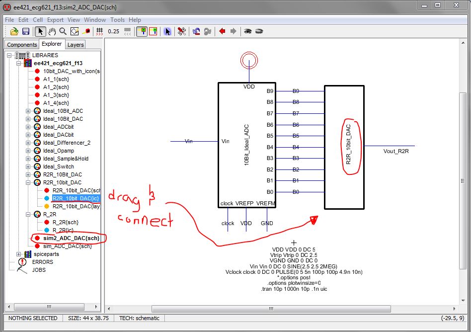
5.)
We will now test our design to see if it functions correctly, we will
first start off by right clicking on the "sim_ADC_DAC" schematic cell
and duplicating it to a new cell called "sim2_ADC_DAC". We will replace
the 10Bit_Ideal_DAC in the schematic with our own DAC icon, by simply
dragging it onto the schematic and wiring it up.By simulating the new "sim2_ADC_DAC" schematic, we get the following results, which means our DAC unit works as expected.
What
happens when we use our DAC to drive a capacitive load of 10pF? We will
modify our "sim2_ADC_DAC" schematic and add a capacitor as shown below
of 10pF.

Here
are the simulation results with a capacitive load, we see that Vout_2R2
starts off at zero and is also lagging Vin. After a few periods, the
wave starts to shift up but still lags the input and is attenuated.
Another good thing to note is how Vout is now smooth due to the
capacitor, as opposed to the "staircase" pattern given before.
If
we now switch the capacitive load to a resistive load of 10K we obtain
the following simulation results. Notice that Vout is half the input
due to the 10k forming a voltage divider with the DAC circuit.

For
our last test, we will put a 10k resistor load along with a 10pF
capacitive load as shown below. Notice how in the results we have the
output smoothed out, is lagging the input voltage, and is attenuated
due to the resistive load component. All these factors should be
considered when using the DAC we designed.


6.) In
a real circuit, the switches that are shown in Figure 30.14, are
implemented using MOSFETS, if the resistance of the switches isn't small
compared to R, then it causes the output to be attenuated by a factor
depending on the size of R.
Backup up my work is shown below, the lab2 file is safely in my dropbox account

Return to EE 421L Labs