Lab Design Project, Part 2 - EE 421L
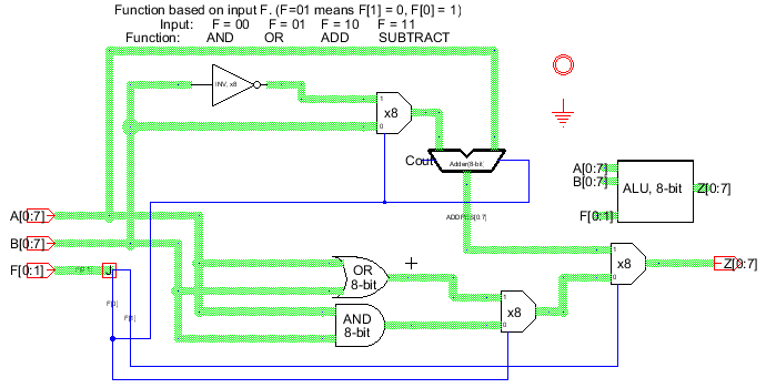
| Input (F) F[1] F[0] | Output (Z) |
| 00 | Z = A AND B |
| 01 | Z = A OR B |
| 10 | Z = A + B |
| 11 | A = A - B |
F[0] is least significant bit, or LSB.
F[1] is most significant bit of control signals (MSB).
For maximum clarity, a second jelib file has been inserted into this
No major changes were made to the schematic, which is presented below for convienience.
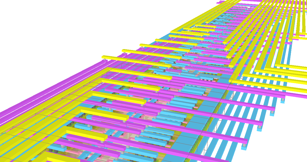
The general layout is presented below:
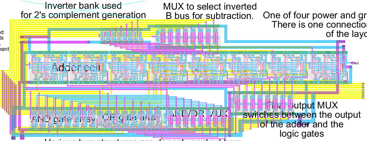
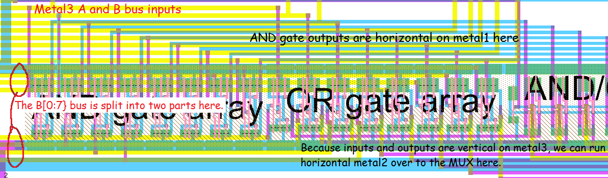
The annotation text is clearer if subcell layouts are hidden when viewing. A few detailed views are presented below.
First, the connections between the AND and OR gate arrays and the MUX that selects the output. Note that the
bus inputs generally run horizontally on metal3, with vertical runs of metal2 for connections into the cells. The leaves
metal1 available for a horizontal bus on the top, and metal2 for a horizontal bus below.
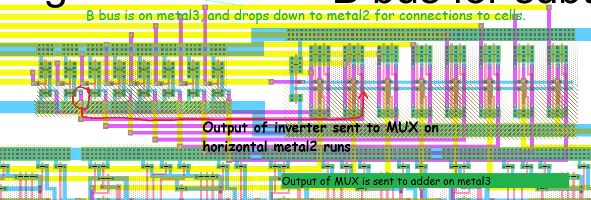
One final region to discuss is the inverter on the B bus before it gets to the adder. As noted in the picture,
the three different layers really help the circuit designer increase density. Obviously, having 6 or 7 layers
would greatly ease the difficulty of routing large 32 and 64 bit busses, and perhaps even leave room for shielding
between layers of so-called "noisy" digital signals.
This concludes our project.
The .jelib file can be found here