Lab 7 - EE 421L
Author: Jason Silic
Date: November 1, 2013
Email: silicj@unlv.nevada.edu
Lab
description:
This lab is an introduction to the circuits used in ALUs. We will work on word size
inverters, Multiplexors, and an adder. The only circuit that we will lay out
will be the adder, but there will be simulations of the other circuits.
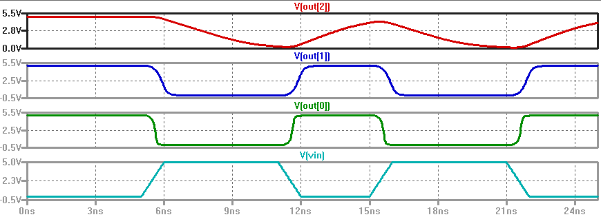
The first circuit we develop a schematic is an eight-bit inverter.
Below is the schematic:
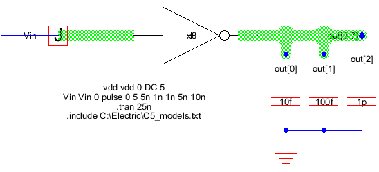
Note the bus connections. We have attached three capacitors of varying
sizes to the first three outputs. LTSpice sim results for this schematic,
inverter_sim_JS_f13, are below.
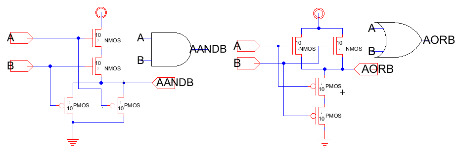
Our next step is to create schematics for NAND, NOR, AND, and OR gates,
and then create bus versions. Our job is mostly done with NAND and NOR
gates from previous labs, so our task is easy. AND and OR gates do have one slight problem.
The most obvious circuit, based on previous design of NAND and NOR gates will
have NMOS transistors connected to VDD, and PMOS transistors connected to ground.
This is a problem for our sframe layout, and a real design may use inverters at the inputs
to sidestep this problem. For our purposes, we are not doing layout, so we will make the circuit
as simple as possible. Below are schematics of the AND and OR gates.
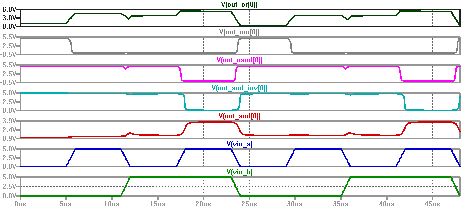
Our simulation schematic is shown below. The waveforms are not very clean.
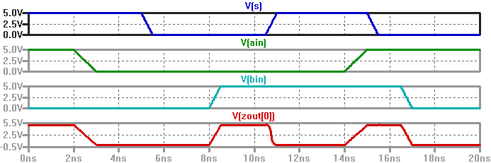
The next circuit is quite interesting. This DEMUX circuit will transmit input A to out put Z when S is high and Si is low.
The NMOS and PMOS transistors connecting A to the output are turned "on" while the transistors connecting B to the
output are turned "off." Below is the schematic.
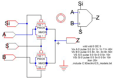
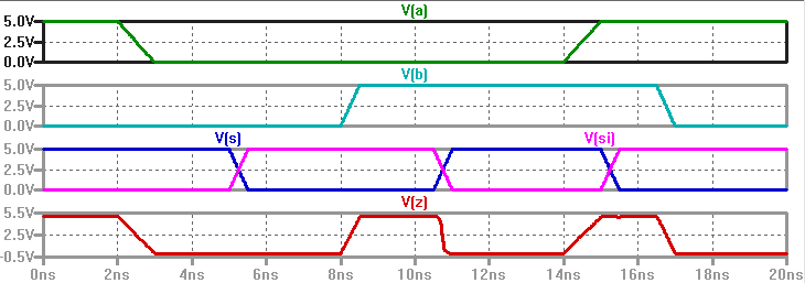
The simulation results are below, confirming the operation of the circuit.
This circuit could also be used as a MUX, if Z was an input and A and B were outputs.
Note that the NMOS and PMOS transistors in the circuit can conduct current in either
direction. This will enable the circuit to be either a MUX or DEMUX.
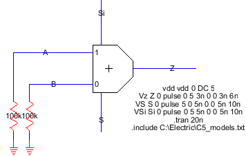
The two resistors pull the A and B outputs low, to make the simulation
easier to understand. Otherwise, the inactive outputs are in a high-Z,
or high impedence state. The below simulation result confirms this.
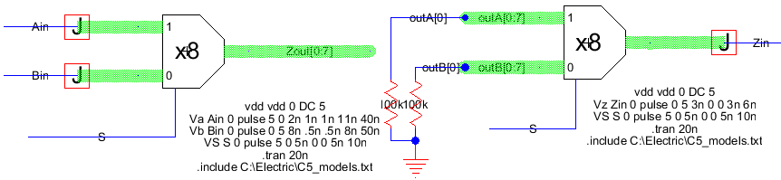
The circuit diagram of the array version of these circuits is below. The two circuits are
MUX_sim_JS_f13(left) and DEMUX_sim_JS_f13(right).
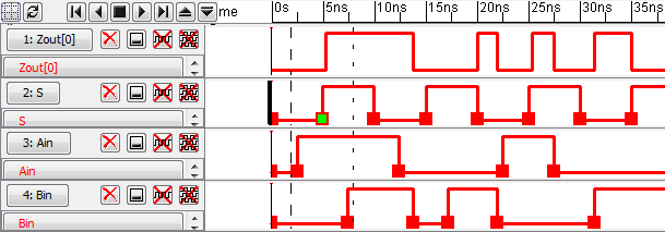
The lab also requires IRSIM results for both of these circuits. Below are the LTSPICE and
IRSIM result for the Multiplexer (MUX) circuit. Again, when S is 1, input A is transmitted to Z,
and B is transmitted when S is low.
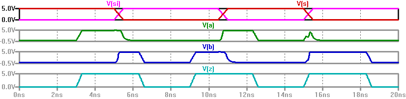
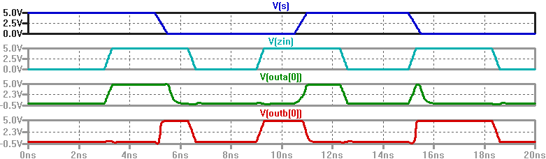
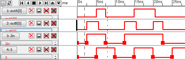
The next two figures are the LTSpice and IRSIM results for the Demultiplexer circuit
with pull down resistors on outA[0] and outB[0].
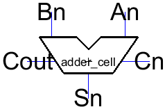
Finally, we draft a schematic of a full adder cell (one bit) using the diagram in the
CMOS book, fig. 12.20.
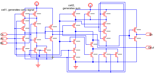
A little modification makes the symbol from lab6 ready for use here.
The array version, or 8-bit full adder is next. Below is the schematic and icon.
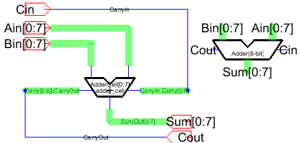
Simulation with IRSIM was hindered by numerous java errors, but eventually it worked.
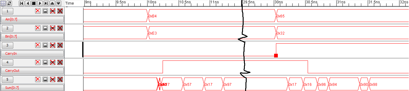
We test the circuit with two different numbers. First we add 180(0xB4) and 227(0xE3),
with CarryIn low. The result is 407, which means CarryOut is high. The remaining 8 sum
bits are 407-256 = 151(0x97). The second calculation is 101(0x65) + 50(0x32) + CarryIn,
and the result is 152(0x98) with carry out low. Note that there is some instability in the
output as the ripple carry adder computes the final sum.
Finally, we do the layout for this adder. Although the layout could probably be done more efficiently,
I am satisfied with the transistor density. Inputs to the adder are generally from the top on Metal2,
while outputs are to the bottom again on Metal2.
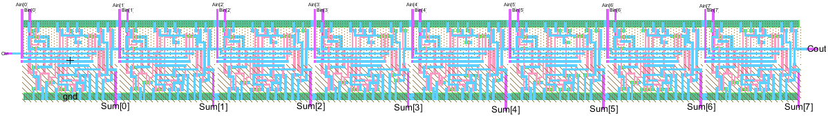
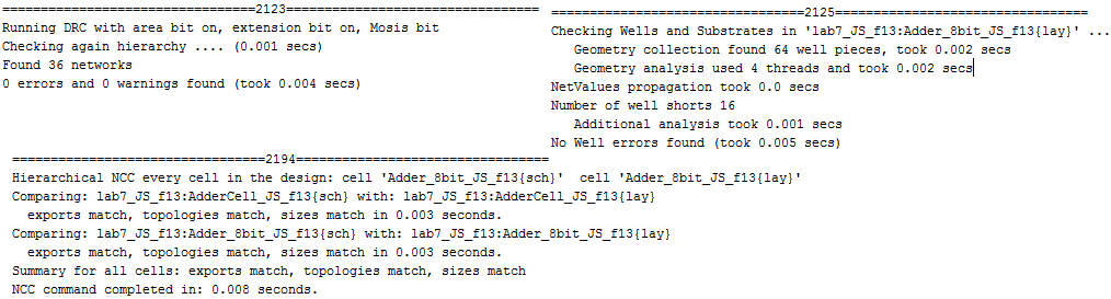
The cell does finally DRC, Well Check, and NCC correctly. (both the individual cell and the 8-bit adder)
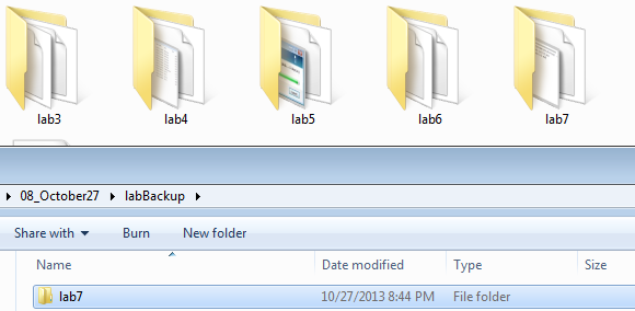
The final step is the backup, as always.
Many of the simulations in this lab can be run easily
with input files located in this zip file.
The jelib file for this lab can be found here.
Return to EE 421L Labs