sframe layouts of NAND2, NOR2, and XOR gates. We will then wire these gates together
with three inverters to create a full adder circuit for simulation. In the final adder circuit
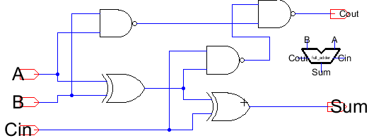
we replace the NOR gate and three inverters with a single NAND gate for our final full
adder schematic and layout with our sframe blocks.
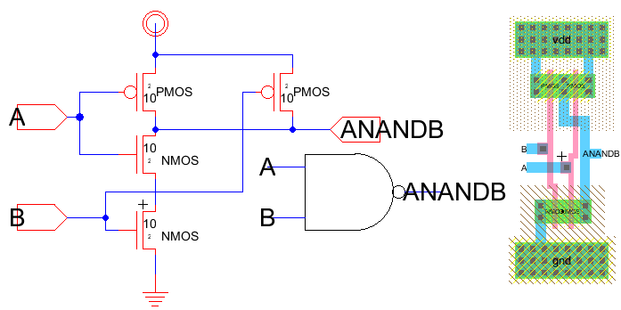
Our first circuit is a two input NAND gate, referred to as NAND2 in shorthand notation.
This schematic and sframe block are named NAND2_JS_f13.
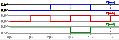
The PSpice and IRSIM simulation results for this NAND gate are below. Note that IRSIM is still
giving me trouble, but at least there is enough correct to get a screenshot.
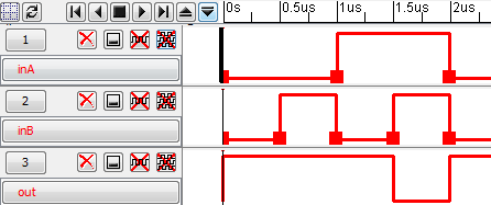
Our next gate is a NOR gate. Below is the schematic (with icon) and layout views.
Note how the later demands of the XOR gate made the sframe for the NOR and NAND
gates a bit larger than they needed to be, but that is a normal result of standard cell design.
This gate uses 20/2 PMOS transistors, in contrast to the previous NAND gate.
PSpice and IRSIM results are below.
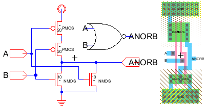
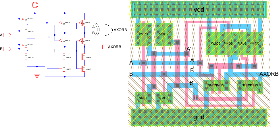
Our final design of a sframe logic block is a XOR gate with two inputs and
twelve transistors. Eight transistors are used for the gate itself, but complemented
inputs are required, so four additional MOSFETs provide two inverters. The layout was quite
interesting, but I finally routed all required connections on only poly1 and metal1. The
sframe is as tall as it is because of the requirements of this gate. The NCC check for this
circuit also required some troubleshooting. When I discovered that two of the inputs to the
NMOS transistors between the output and ground were reversed, I changed the schematic
instead of the layout, as that is a lot easier.
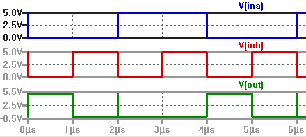
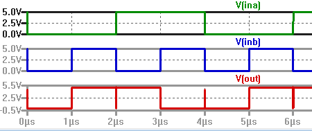
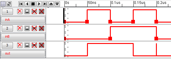
Simulation results are below. Note the transients in the PSpice simulation (and IRSIM as well).
This design certain is not extremely high-performance!
Next the first adder circuit with three NOT gates is designed and simulated.
The schematic is quite messy with so many gates.
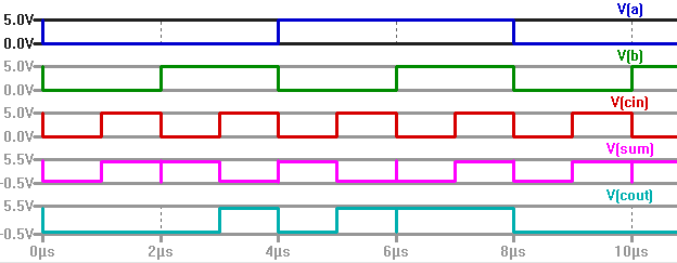
PSpice again shows the correct operation for this circuit.
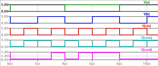
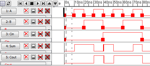
IRSIM, after the usual complaining, produces much the same results.
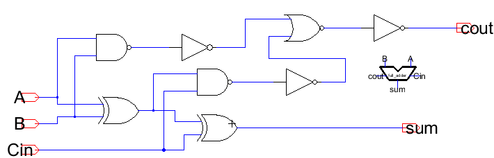
As noted in the lab instructions, we can simplify this circuit by noting that the
NAND function (AB)' = (A' + B'), which is the OR function with inverted inputs
by De Morgan's Law. These inversions cancel the inversion at the output of the NAND
gates in the previous stage, resulting in AND-OR combinational logic. Schematic below.
Note that the inputs to the gates are sometimes reversed. This was to match the schematic with
the layout during the NCC process.
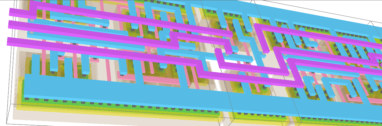
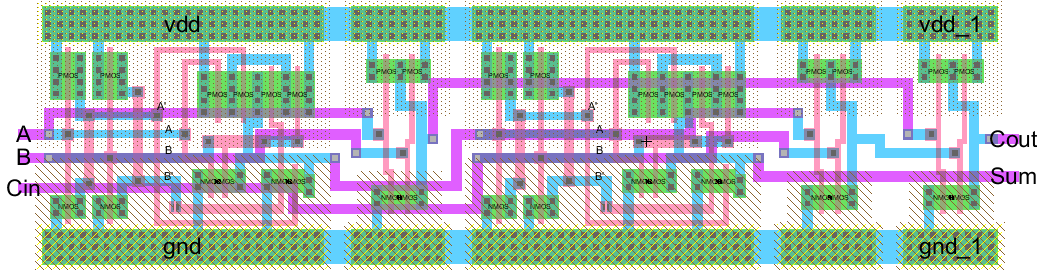
The layout itself is perhaps the most exciting part of the lab, as the routing
of all the connections was quite the challange.
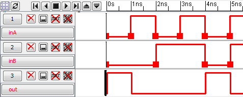
The simulation results for this circuit are similar to the results from the last circuit.
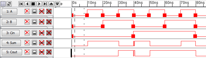
IRSIM provides the final simulation result:
A quick backup of the folder helps to prevent accidental deletion: