Lab 5 - EE 421L
Author: Jason Silic
Due: October 4, 2013
Email: silicj@unlv.nevada.edu
Lab
description:
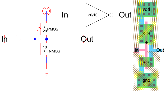
This lab will give the student experience with inverters using CMOS technology.
We will create schematics, icons, and layouts for an inverter with a 20/2 PMOS
and 10/2 NMOS transistors (this is the 20/10 inverter). then we will create
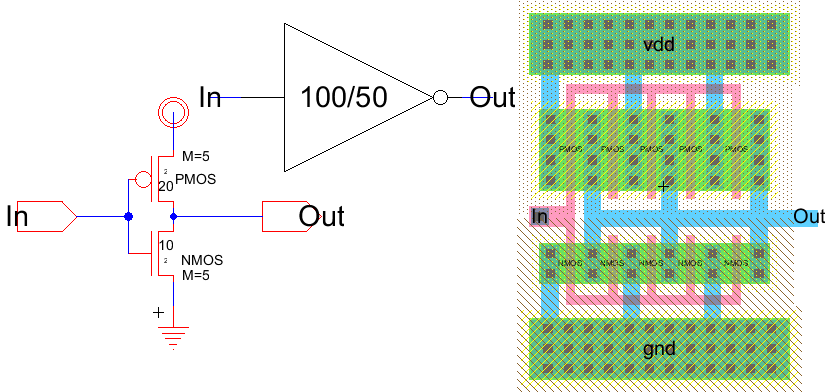
a 100/50 inverter, by using five transistors instead of one. The reason we use
five transistors is to give the inverter more driving power, which will lead to shorter
rise times when connected to capacitive loads. This will become obvious in our simulations.
Our first step is to build the NMOS inverter. Below are the schematic with icon and the layout.
The PMOS inverter is similar. Note the "M=5" text that indicates the multiple transistors.
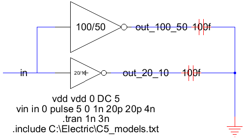
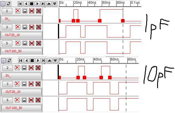
Our next step is to simulate these inverters with SPICE. This basic circuit it used, with three different version.
One has the inverters driving 100fF loads, and the next two have 1pF and 10pF capacitors.
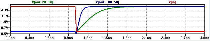
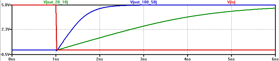
Here is the simulation results with a 100fF load. Note that the 100/50 inverter has a much faster response time.
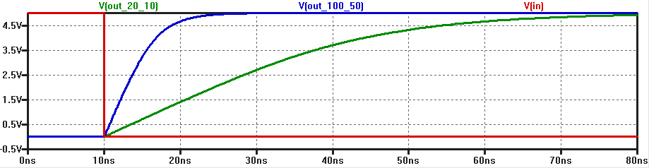
In the second simulation, with a 1pF load, the time delay increases substantially (approximately a factor of 10).
When the capacitance is increased again by a factor of 10 to 10pF, the delay increases as well.
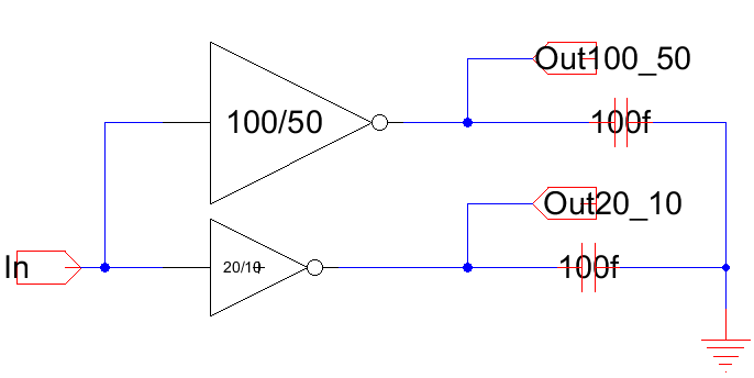
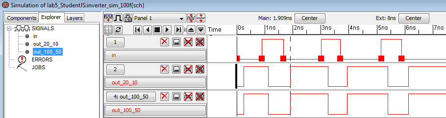
Next we use the ALS simulator to simulate our inverters. ALS requires input and output ports to create a VHDL file, so we
modify our schematics to include these. Here is the 100fF cell:
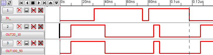
Our ALS simulation does not seem to take into account the difference between the 100/50 and 20/10 inverters.
This is not surprizing as ALS is a logic simulator. Note that the delay is a constant 10ns in the output below:
When the capacitive load is changed to 1pF and then to 10pF, there is no noticeable change.
The delay remains fixed at 10ns.
The above outputs demonstrate the limitations of ALS. The simulation does not take
into account the load capacitance and will thus not expose any problems in a circuit that
are the result of excessive delay. Any transistor is considered sufficientOur next simulator, IRSIM, does model transistors to some extent, so we expect results
that will reflect the differences between the inverters and also the changing load.
Note that to create the input waveforms for both ALS and IRSIM, the process is to
select the input wave, move the "main" cursor to a point on the waveform and then
set the waveform to either low or high. The shortcut keys for this are "G" and "V."
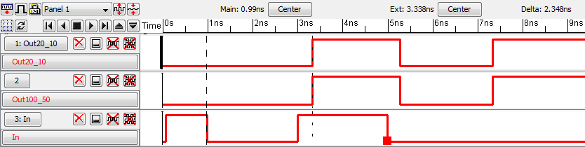
Below are the results with load C = 100fF.
The
next one with a load of 1pF gives a delay 10 times as long (~2.3ns).
Note the Delta between the Main and Ext cursors is 2.348ns.
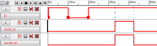
The final circuit, with a load of 10pF has a delay of approximately 23ns, and the very important zooming feature is
required to view the entire waveform.
IRSIM was able to simulate increasing delays with increasing capacitive load, but was not able to differentiate the
two different types of transistor that we used. This could be because our schematics are designed for LTSPICE, and
IRSIM might have had some difficulty reading the appropriate information.
LTSPICE seems easier to use, and also more accurate, but this may be because the Professor has spent so much
time teaching us how to use it.
The jelib file for this lab can be found here.
I have backed up the first five labs to an external hard drive:
Return to EE 421L Labs