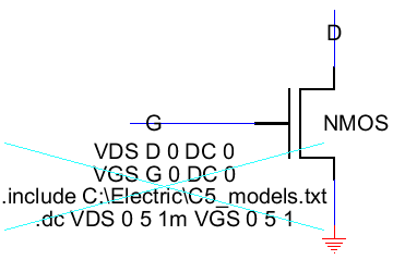
the insertion of the NMOS symbol, off-page connectors, and connecting wires. Then the off-page
nodes were exported with symbols such as G for the gate connection. Perhaps the most imortant step
was selecting the transistor and setting the SPICE code to "NMOS" to use the model from C5_models.txt,
which we reference in the simulation files. Next it was a simple matter to draw a crude icon to represent
the transistor more effectively in a larger schematic, and this is shown below with NMOS schematic.
More detail on the icon process will be provided in the PMOS section, as the two are similar.
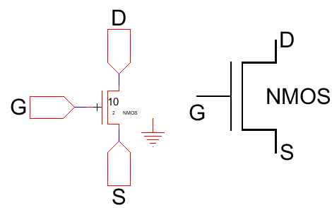
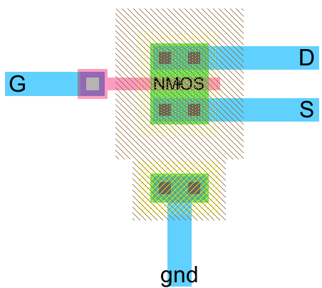
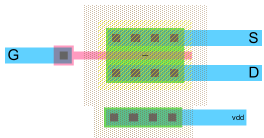
The layout of the NMOS is quite simple, with a channel width of 10. Note that the body connection
is tied to ground, and the gate, drain, and source are exported with appropriate names to match the schematic.
The PMOS transistor is very similar to the NMOS. Our procedure is basically the same,
but I do want to go over the icon creation process. The hardest part is remembering to
view the schematic and the do the command View->Make Icon View. This create an icon
to go along with your schematic. The only other thing is to also remember to put
export->wire components in your icon to provide connections. Here is the PMOS
schematic and layout. Note the power connection in the schematic to make the schematic
match with the layout, which requires a power connection to the body. This is the same
reason that the NMOS schematic had a ground connector.
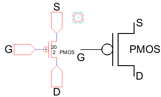
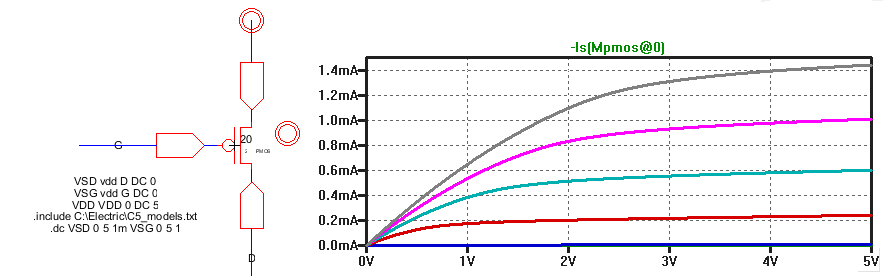
Note the greater width of the 20/2 PMOS transistor, to compensate for reduced
p-type silicon hole mobility.
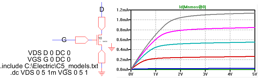
Finally we make simulations using our NMOS and PMOS transistors. Below is a composite picture
of the NMOS simulation schematic and the simulation results (.plt file is here)
The PMOS is similar, and the increased width actually gives it higher current than the NMOS: (.plt file is here)
Finally, incorporating an icon representation into your schematics is quite simple: place the icon and connect wires
to the exported pins, as shown here:
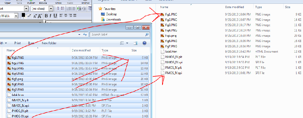
The jelib file for this lab can be found