Lab 3 - EE 421L
Our first step is to lay out 10k n-well resistors. The latest data from MOSIS indicates a sheet resistance of 800 Ohms/Square.
A simple calculation indicates that we need resistors 12.5 squares long. With a minimum width of 12 lambda, this is a length of 150 lambda.
Electric measures the length of the n-well resistor from the contacts, to the actual structure is a little bit longer than the nominal length.
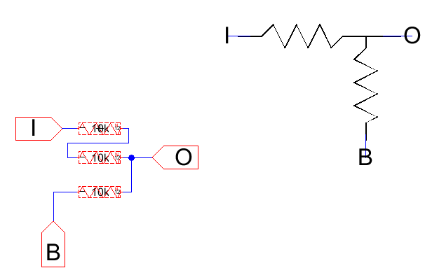
Our complete schematic is mostly made up of a repeating pattern of three resistors, whose schematic, "R3_UnitCell," is shown below.
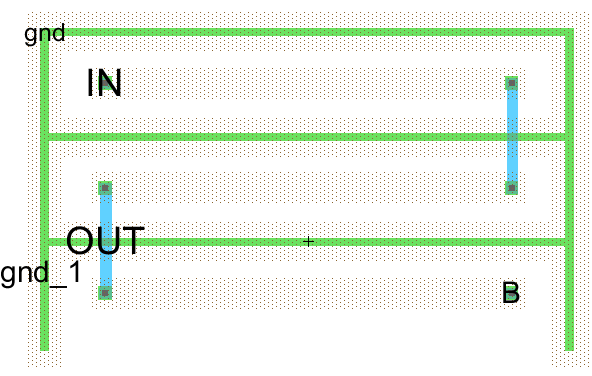
Our layout of this cell includes three n-well resistors, stacked as directed. Note the p-active
"ring" around each resistor that helps prevent fluctuation in the potential of the p-well.
Our final circuit is simply ten of these cells, stacked and connected appropriately.
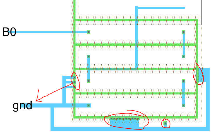
As the professor noted, the n-well that the p-active pin seems to create has to be
grounded as well as the p-active strip. This is shown here with the extra resistor needed
at the bottom of the resistor ladder in the DAC.
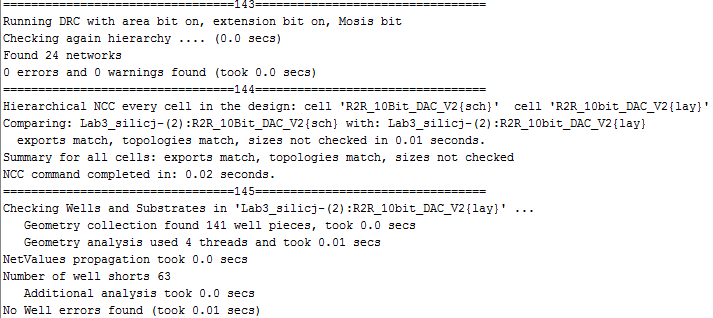
After the above design was complete, there were no layout errors (or DRC errors), the NCC showed that
the layout matched the schematic, and the ERC well check was also passed.
The jelib file for this lab can be found here.
The spice file to make the plot appear automatically is here, simply save to the same directory as the .jelib file.
Of course, all of this work is backed up in a few different places. Here is my backup folder with the last few labs: