Lab 2 - EE 421L
Author: Jason Silic
September 6, 2013
Email: silicj@unlv.nevada.edu
Lab
description:
This lab introduces the student to the basic operation of Digial-to-Analog converters (DAC) and the inverse device,
the Analog-to-Digital converter (ADC).
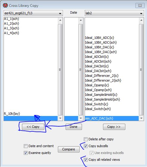
Our first step is to import a library with the schematic of a circuit that converts a sinusoid analog input to a digital
intermediate stage and then back to an analog signal. As seen below, a cross-library copy gets the job done.
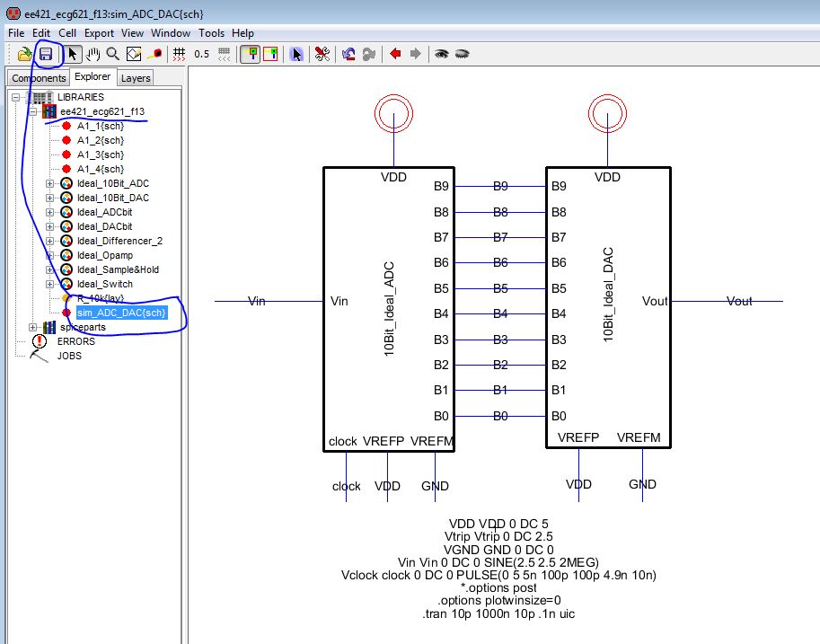
When the "sim_ADC_DAC" schematic is opened with Electric, a block diagram view is presented.
Also, the .jelib library can be saved at this point and backed up by an appropriate method.
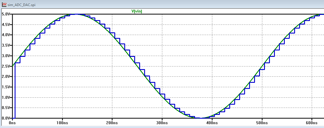
Simulation results show the clocked nature of the ADC, but with ten bits of accuracy, we don't really get to see the discrete
voltage
levels produced by the digital conversion. 2^10 is 1024, so there is a
discrete voltage level approximately every 5mV.
(actually it is 5/2^10 = 4.88mV) Such finely quantized values are not visible on the graph, and we instead see the clock pulse
updating the output of the ADC every cycle.
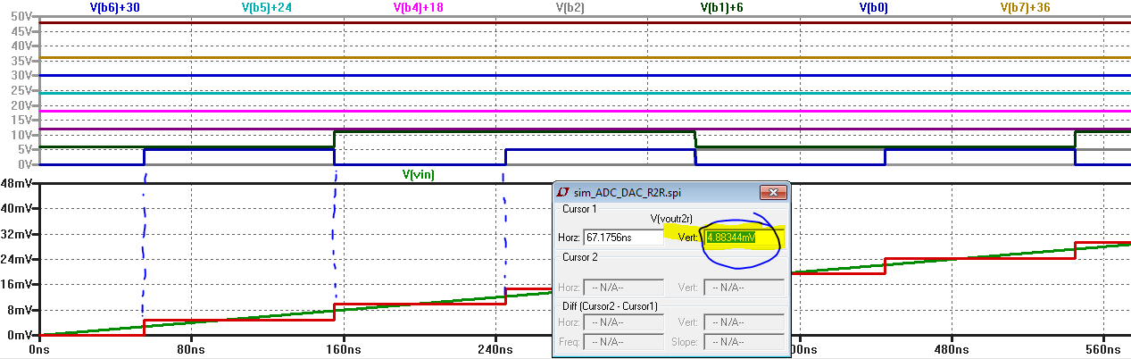
In
order to determing the least significant bit (LSB) and most significant
bit (MSB)
of the the DAC, we can introduce a ramp function to the input and examine the bits
B0-B9 to determine that B9 is the MSB and B0 is the LSB. Also, from the graph
below it is clear that the discrete change in voltage from one level to another is
about 4.88mV. This is the minimun voltage needed to produce a change in the output
of the ADC, and is referred to in the lab manual as the LSB voltage, I think.
We
see in the above picure the basic operation of the ADC and DAC. Note
that the a 10-bit digital signal can have only 2^10 = 1024 distinct
states.
The ADC chooses the digital signal which represents the voltage level
closest to the input voltage. The DAC then will convert this digital
signal
into an output voltage. Considering a 10-bit DAC here, the output
voltage is [(Vmax - Vmin)/(1024)]*Input, where Input is the binary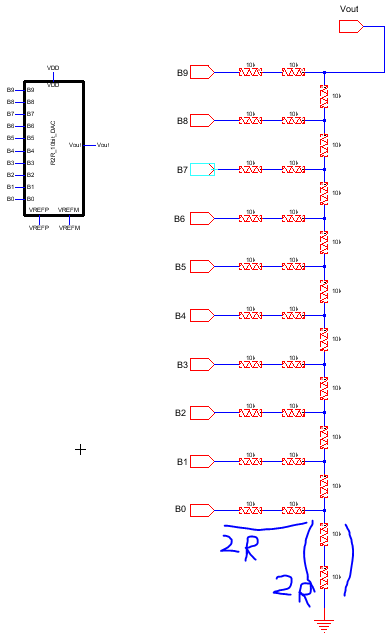
number
from 0-1023 represented by the digital signal lines. Note in the above
capture that the red graph in the lower set of axes is the
output of the DAC.
PART 2: BUILDING AND TESTING A RESISTIVE DIGITAL-TO-ANALOG CONVERTER
In this section we first construct a resistor network that acts as a DAC, as seen below.
The simulation results are very similar to those for the ideal DAC, but there is no load yet.
To determine the output resistance of the DAC, note that the last set of resistors at the bottom
are in parallel, as seen at right. Combining 2R and 2R resistanced gives us a resistance of R,
which combines in series with the resistor attaching to the next node above to give equivalent
resistance to signal ground 2R. The process then repeats to the top of the network, and the
final output resistance is R.
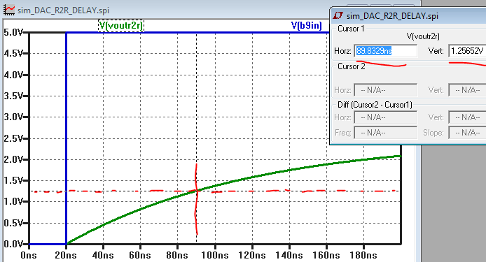
The next step is to determine the output response with a 10pF capacitor attached to the output.
With an output resistance of R (which is 10k in our case) attached to a capacitance of C,
the time delay to reach half of the full output voltage should be approximately 0.7RC.
In our case this is 0.7*10k*10p = 0.7*100*10^3*10^-12 = 70ns.
In the simulation results seen below, this appears to be accurate, as the output voltage
reaches half of the final value of 1.25V (2.5V/2 = 1.25V) at approximately 90ns, which
is 70ns after the pulse at 20ns. Note that final voltage is 2.5V because only the most
significant bit is active, and that represents about half of the total input range possible.
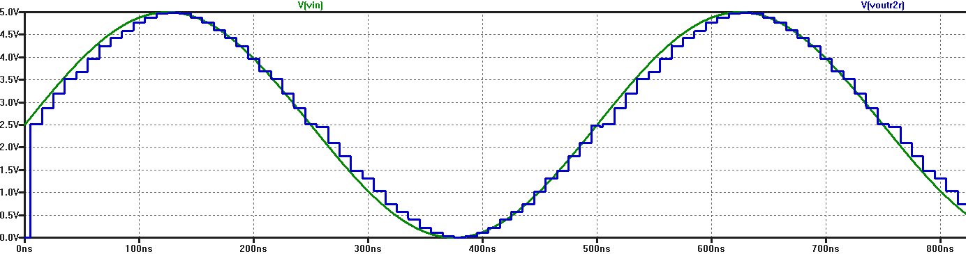
Now we show this resistor network DAC with its own symbol and test it out in the original circuit.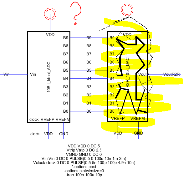
As noted above the results are indistinguishable with no load, and we will present simulation results.
To set up a sub circuit's visual representation, simply go to the 'ic' file in the explorer and start
placing components. With a little work you can get some interesting line art going, but the results
are probably not very descriptive of how the circuit works.
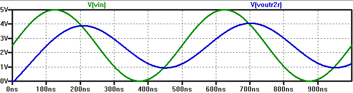
Regardless, the below simulation results clearly indicate that the circuit is working properly.
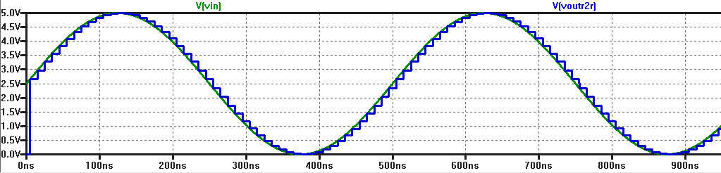
If the DAC drives a capacitive load the output waveform is phase shifted:
If
there is also a resistor then the output voltage becomes "stepped"
again, as the output voltage is not directly smoothed by the capacitor.
The following graph is optained with R = 10k, C = 10pF.
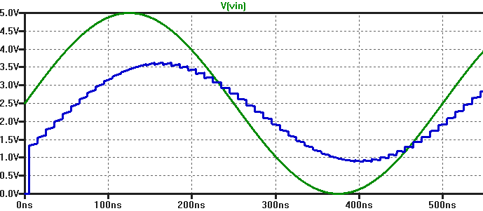
Finally, when the output resistance is 10k, the output voltage is essentially half of what it should be
because the output resistance and the DAC's internal resistance form a voltage divider so that only
half of the voltage appears at the output terminal.
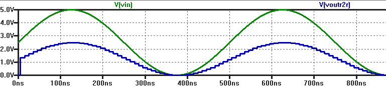
When additional resistance is introduced into the input of the DAC, possibly from MOSFET driver transistors,
the resistor network changes. The output range of the entire DAC drops, because more voltage is dissipated
in the input drivers than the design is prepared for. The high-order bits probably have the most relative gain
in influence, and loose the least of their effect on the output voltage, because they have the most direct access
to the output. A simulation with an extra 5k resistance added to the input is shown below. Note that the
output waveform is a bit unstable.
Return to EE 421L Labs