Lab 1 - EE 421L 


By Jason Silic

August 30, 2013

Email: silicj@unlv.nevada.edu


Lab description:

In this lab, the student becomes familiar with the Electric CAD tool through a simple tutorial.


Figure 1 is the first screen you see on starting Electric:


snip1


Figure 2 is the result of changing the background to white:


snip2


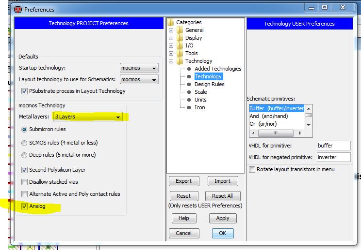
Fig. 3 shows how to set up Electric for the "ON semiconductor's C5 process," with three metal

layers and the "Analog" option selected.


snip3


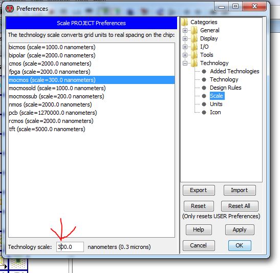
The next step is to set the "lambda" constant, which for our case is 300nm. (Fig.4)


snip4


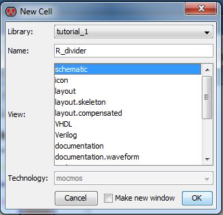
The next step is creating a new "Cell," and the following dialog box pops up. (Fig. 5)


snip5


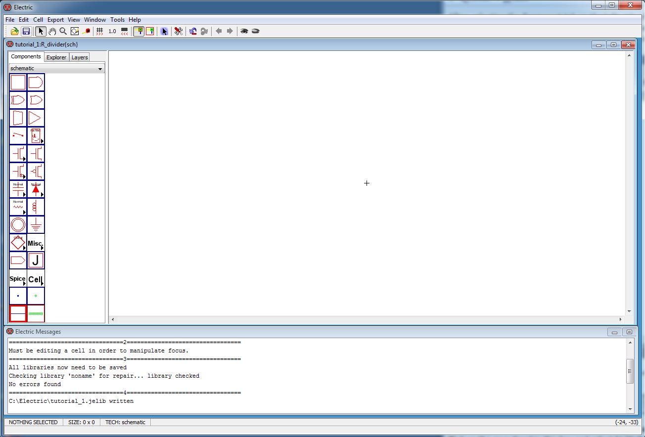
We get this screen, ready for components to be placed. (Fig. 6)


snip6


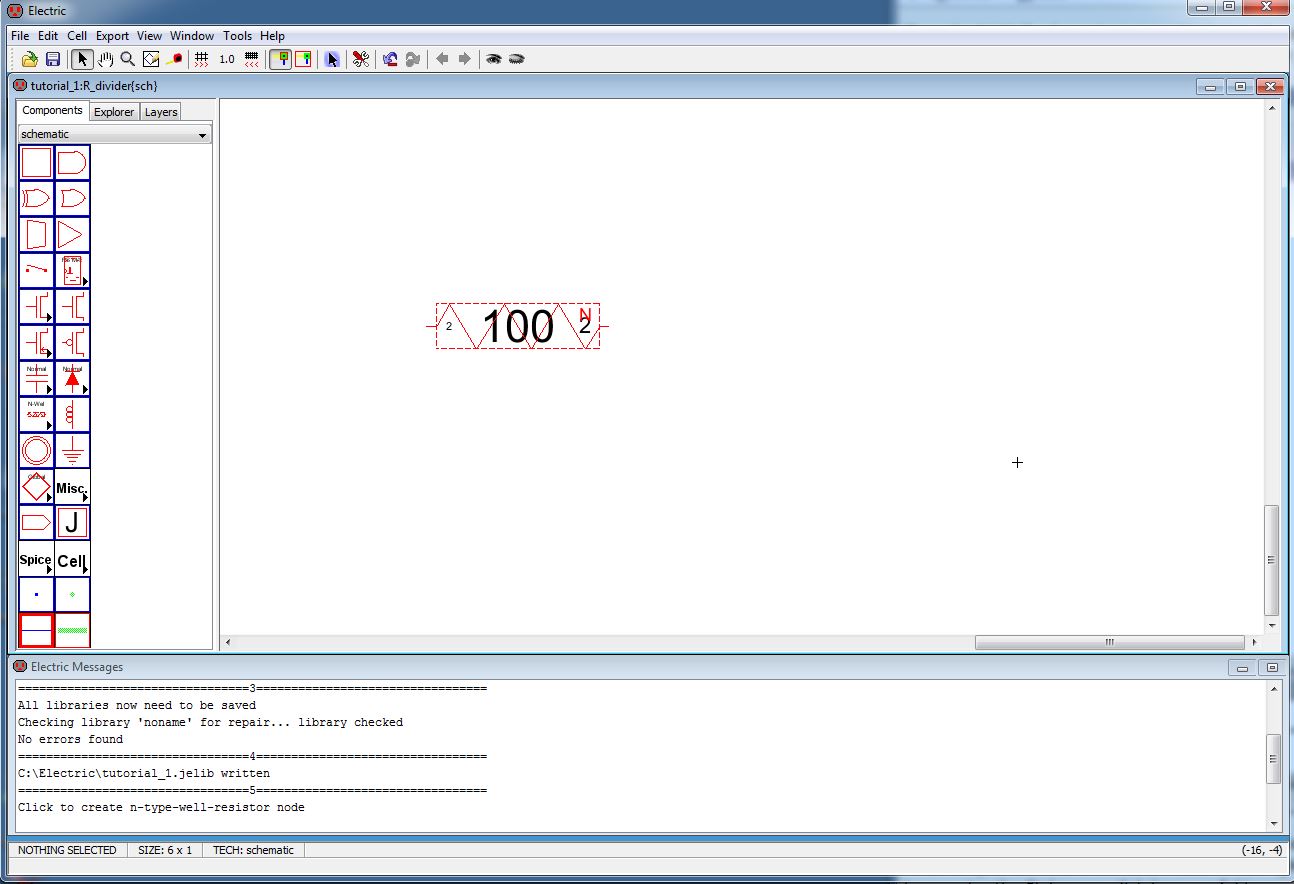
Now we place a so-called N-well schematic resistor "node." (Fig. 7)


snip7


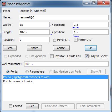
We then set some properties for this node. (Fig. 8)


snip8


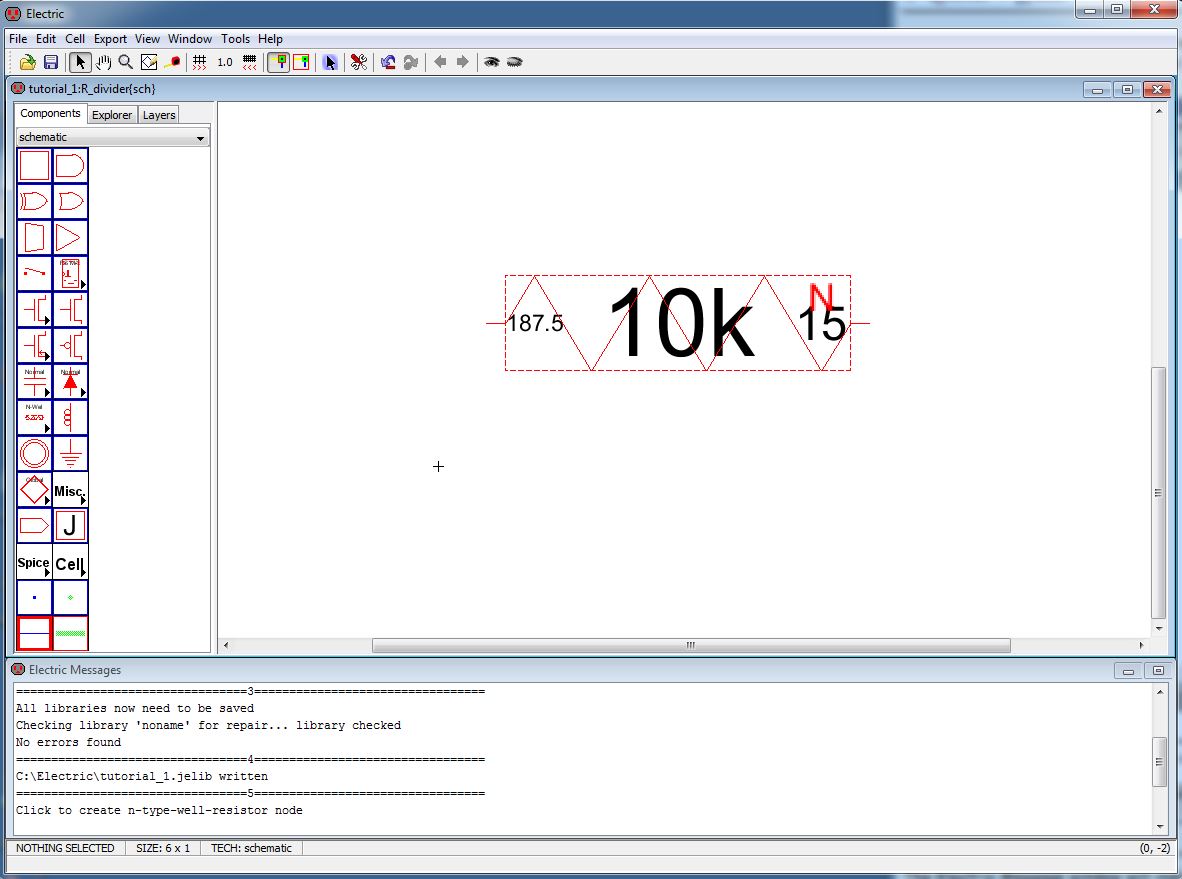
After finishing this step, and zooming in a little, we get this image. (Fig. 9)
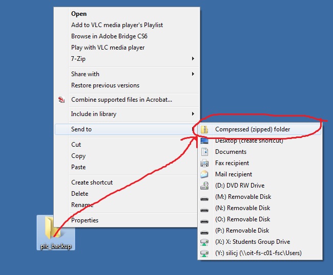
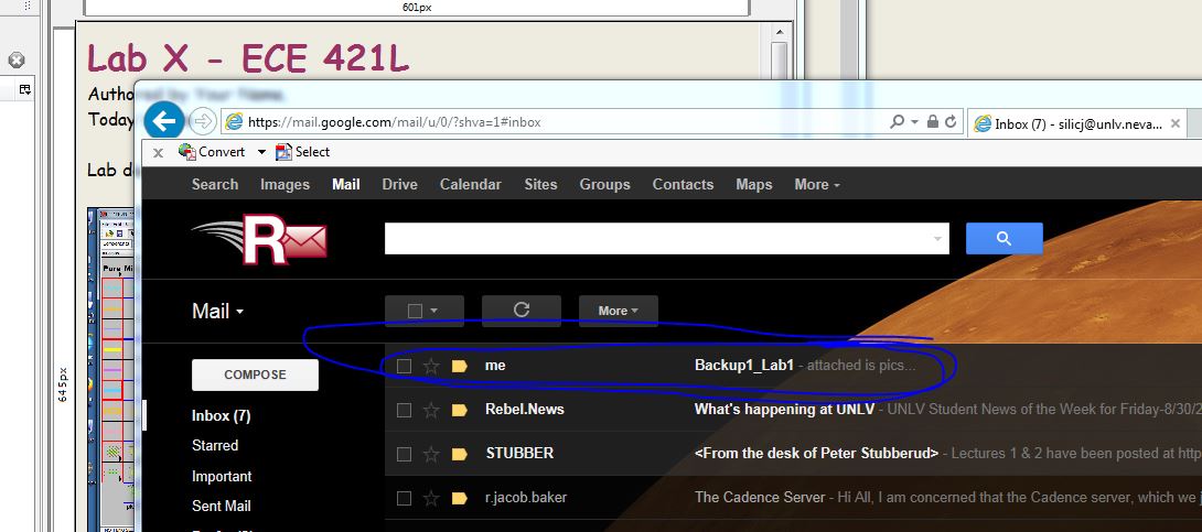
 

snip9


Backup

 
During the creation of these web-based lab reports, it is important to backup your work.
One thing that I did is emailing myself the .jpg files before I started on the html editing,
so that even if disaster struck later, I would still have the first step done. (Fig. 10)
 
Backup1
 
 
The same procedure can be followed for the .htm files.
Fig. 11 shows the email securely stored (I assume) on the Google servers.
 

backup2 


Return to EE 421L Labs