Lab 6 - ECE 421L
Authored
by Matt Mumm, mummm2@unlv.nevada.edu
Today's
date 10/18/2013
Lab
description
We will be building a two input full adder with different logic gates.
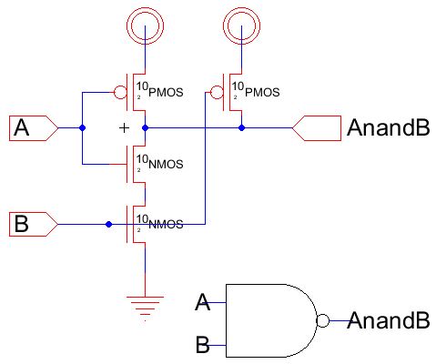
NAND Gate
This is the first logic gate we will be making. It consists of 2 (10/2) PMOS and 2 (10/2) NMOS. Make sure to set the spice model on the devices. Configuration can be seen below.
Schematic
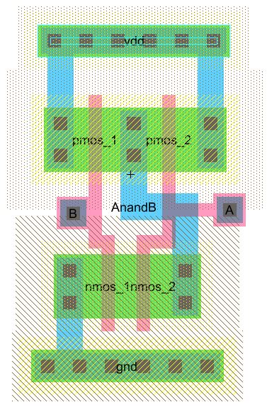
Layout
Notice
that the connection between the two NMOS, there is an absence of N+ to
M1. This is due to the lack of any other connection between the
two.
Simulation
Using spice code and a seperate schematic with the icon, we can simulate the NAND output.
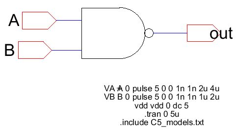
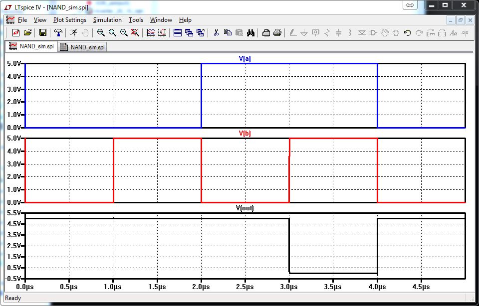
LTSpice
IRSIM
NAND output is 1 only when both inputs are set to 0, otherwise its 0.
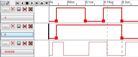
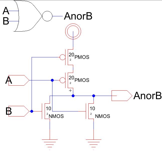
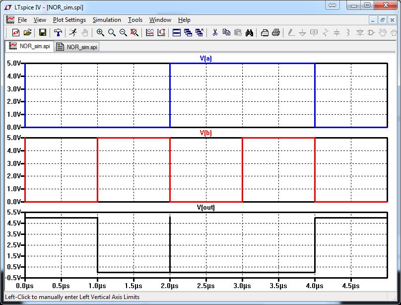
NOR Gate
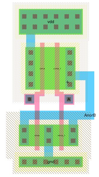
This gate consists of 2 PMOS (20/2) and 2 NMOS (10/2) in the follow configurations.
Schematic
Layout
Simulation
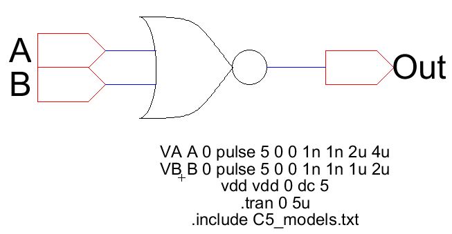
LTSpice
IRSIM
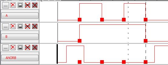
NOR out is 1 when both inputs are 0, otherwise its 0.
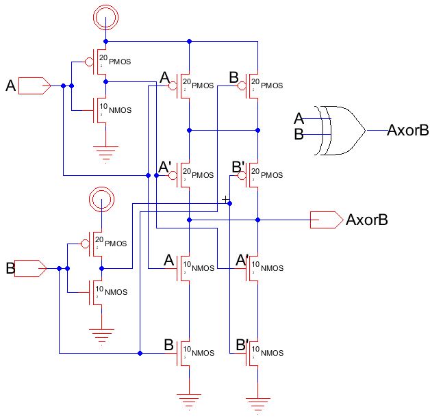
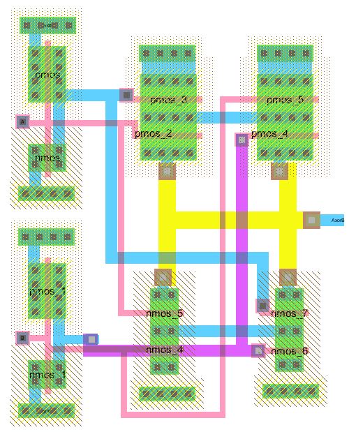
XOR Gate
XOR gate uses 2 inverters (from previous lab) and then 4 (20/2) PMOS and 4 (10/2) NMOS in the following configuration.
Schematic
Layout
Simulation

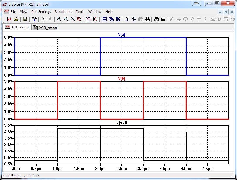
LTSpice
IRSIM
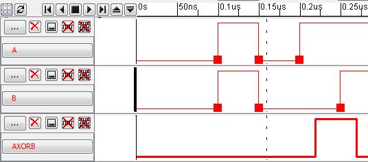
XOR output is 1 when only one of the inputs is 1, otherwise its 0.
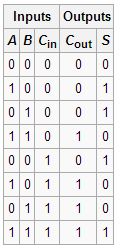
Full Adder
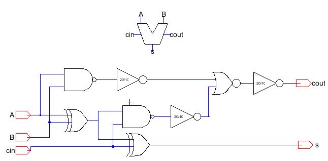
This is the first full adder and it uses 2 NANDs, 2 XOR, 3 inverters and 1 NOR.
Schematic
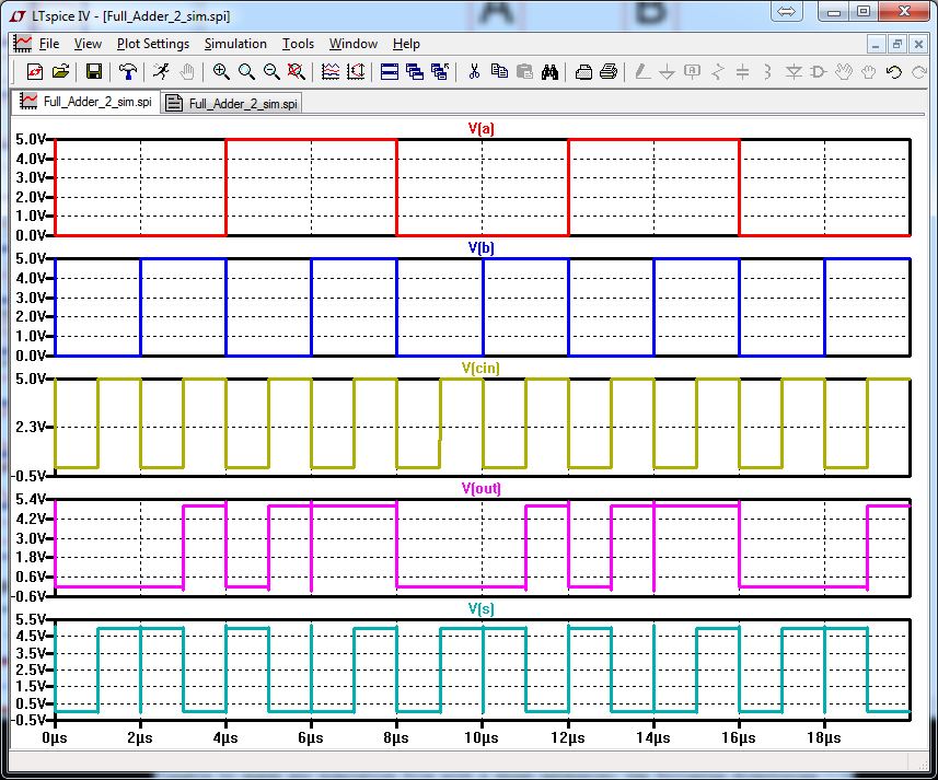
Simulation
LTSpice
IRSIM
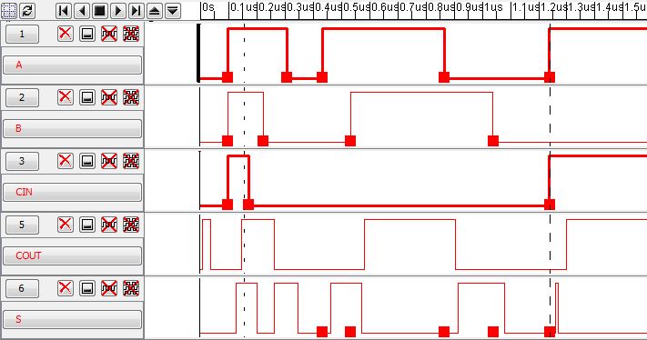
The output is as follows
Be sure to backup your files.
My Lab6 File More information can be found at cmosedu.com