Lab 5 - ECE 421L
Authored
by Matt Mumm, mummm2@unlv.nevada.edu
Oct 5, 2013
Lab
description
We
will be making and testing inverters using the NMOS and PMOS from the
previous lab. We can get a good idea of how much of a time delay
there is.
Inverter:
- Create a new cell schematic.
- Place down PMOS and NMOS device.
- Set the PMOS width/length to 20/2. Set NMOS to 10/2.
- Connect the two together vertically.
- Tie a power source to the unconnected end of PMOS.
- Tie ground to the unconnected end of NMOS.
- Connect the gates together and add an input to that connection.
- Finally tie an output to where the MOSFET devices meet.
The inverter should look something like this.
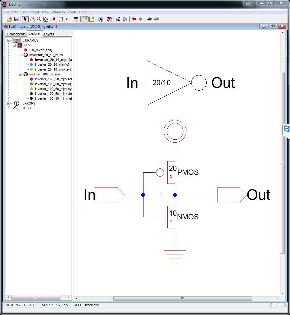
**Also notice that I created an icon for my inverter and labeled it appropriately.**
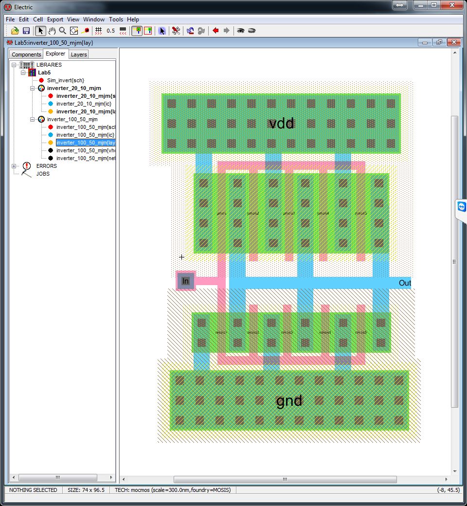
- Create a new layout cell with the same name as your schematic so everything can be grouped together.
- Place down a PMOS with pActs for the source and drain. Change the size to 20/2.
- Place down a NMOS with nActs for the source and drain. Change the size to 10/2.
- Connect
the poly, or gate, together from each device for an input connection.
Connect this to a Poly1-M1 con. Export this with the same name
you used in your schematic for the input.
- Place a nWell above your PMOS device; this will be used as your power source. Connect this to your PMOS via M1.
- Place a pWell below your NMOS device; this will be used as your ground. Connect this to your NMOS via M1.
- Finally,
connect the open connections from NMOS and PMOS together via M1 and
create an output. Label this the same as your schematic output.
You're layout should look something like this. 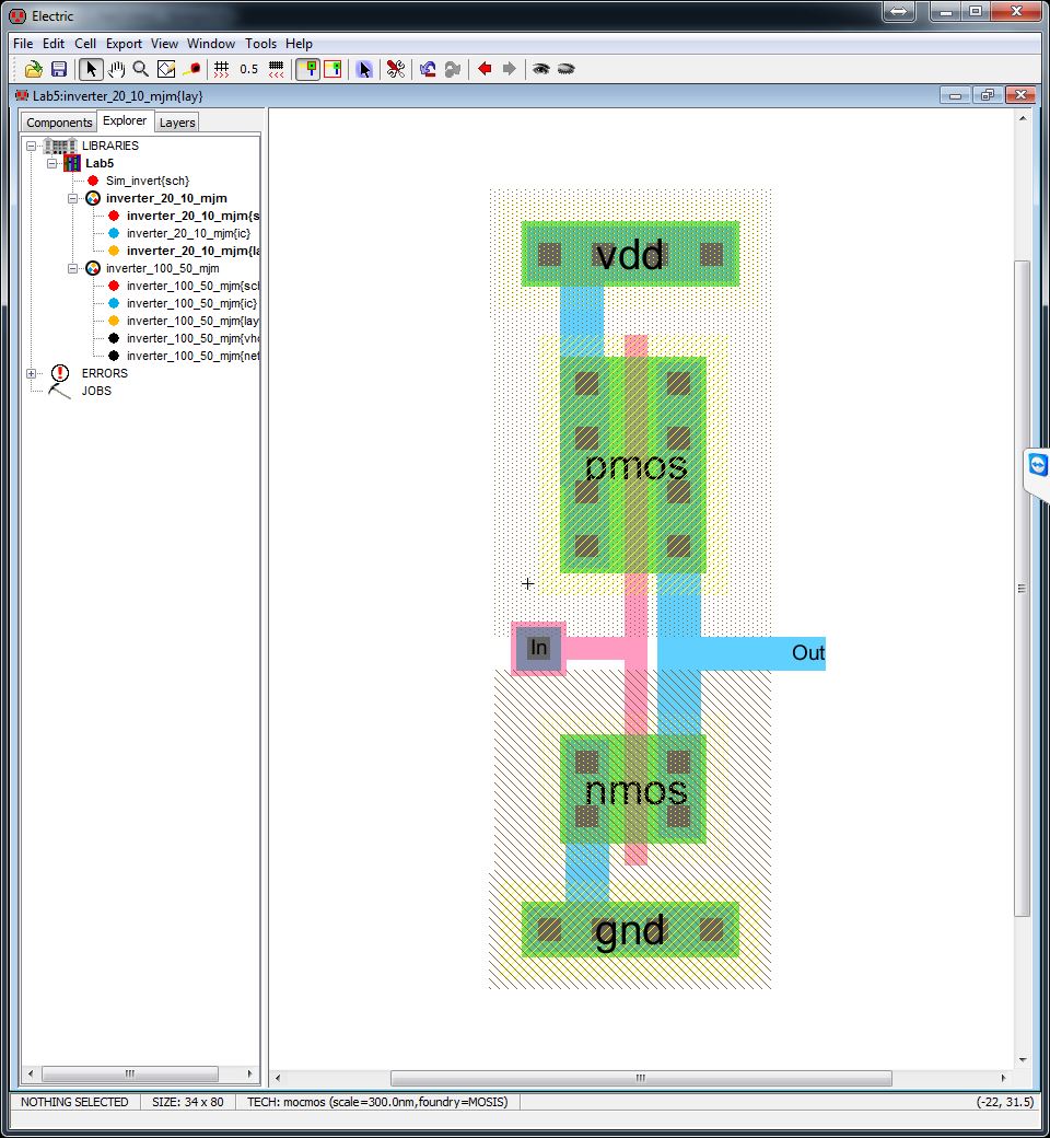
**Now is a good time to check for errors. DRC, Well Check, Layout vs Schematic **
Parallel Inverter
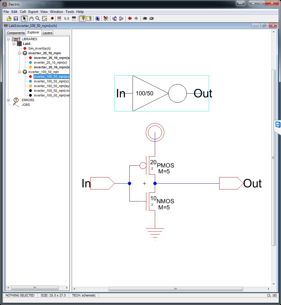
- Right click on your cell group and click "duplicate cells in this group"
- Instead
of placing 5 different transistors in parallel on your schematic, we
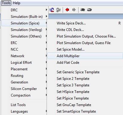
are simply going to multiply them. Select your MOSFET device, go
to Tools -> Spice (Simulation) -> Add multiplier. (See
picture below the schematic)
- Click
on the M that appeared and change the value to 5. We have just
made it so that there 5 MOSFET devices in parallel
- Do the same for your other MOSFET.
- Be
sure to change the name that appears on your icon so we can tell the
difference between the first inverter that was made and this one.
- Click in your new duplicated layout.
- If
you look at the picture below, you will notice that we cannot simply
just add in some code to represent a multiplier. You can however
copy/paste the poly and its right connection to add another MOSFET
device.
- After we have 5 of each MOSFET, we need to reconnect the power, ground input and output.
- All of the polies are connected together via poly1 for the input.
- vdd has been extended and made larger so that it can properly supply power to the MOSFETs.
- ground as also been made larger to connect all the MOSFETs.
- We could also just have 3 different vdds and 3 grounds.
- Finally all the outputs are connected together via M1.
**Make sure you check for errors**
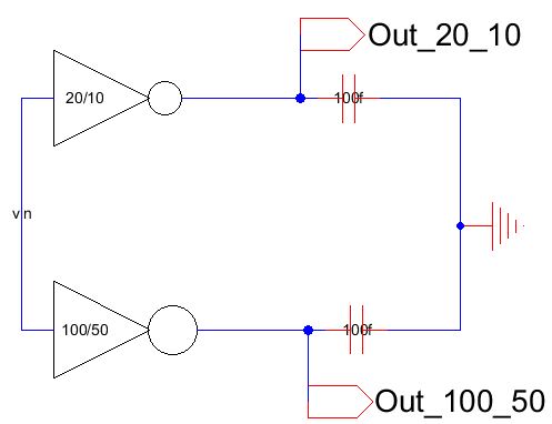
We are now going to check for how long the delay is when connecting to different capacities for each of the inverters.
- Create a new schematic cell for simulation purposes.
- Place each of your icons into the cell by dragging and dropping.
- Connect the inputs together.
- Place a capacitor after each inverter and tie ground to the other side of the capacitors.
- Finally
place an exported output between the output of the inverter and input
of the capacitor. (Plotting is based your off page nodes which
are exported.)
- We will be setting the capacitor values to 100fF, 1pF and 10pF.
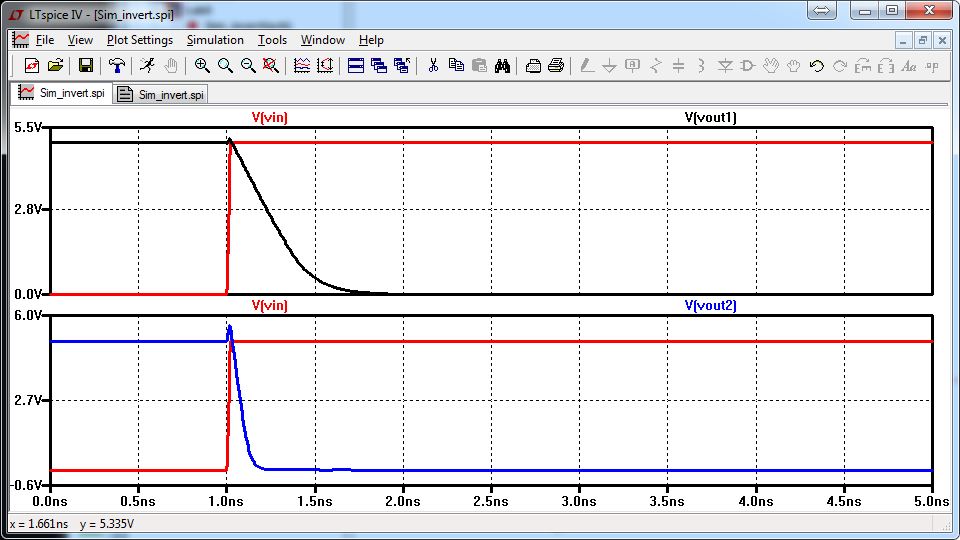
- Write
spice code for the vin as a pulse signal from 0 to 5 in 1ps.
Transient analysis with maximum run time of about 60ns.
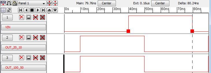
- The second simulation is with no spice code and using Tools -> Simulation (Built-in) -> ALS.
- Selecting
your vin and hitting v or g will change the input signal to high or
low, respectively, at wherever the thicker black dotted line is.
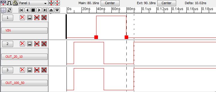
- Look
at the simulation results for cap=1pF. It was dropped from high
to low at about 80ns and then the inverters responded about 10ns
later.
- The difference can be seen in the upper right that is labeled delta. (10.02ns)
- Take note that the delay DOES NOT change with different capacitor loads.
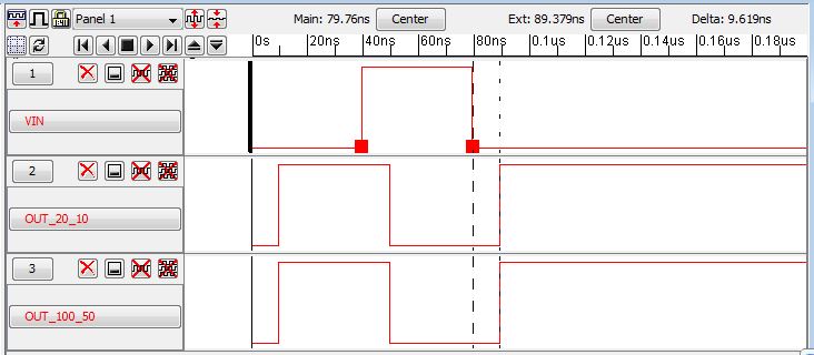
- The third set of simulations is done through IRSIM.
- You will need to add in IRSIM into electric. Please go to here. Step 12
- Go to Tool -> Simulation (Built-in) -> IRSIM: Simulate Current Cell
- IRSIM works much like ASL in respect to hitting v and g.
- The time delay DOES change with capacitor loads.
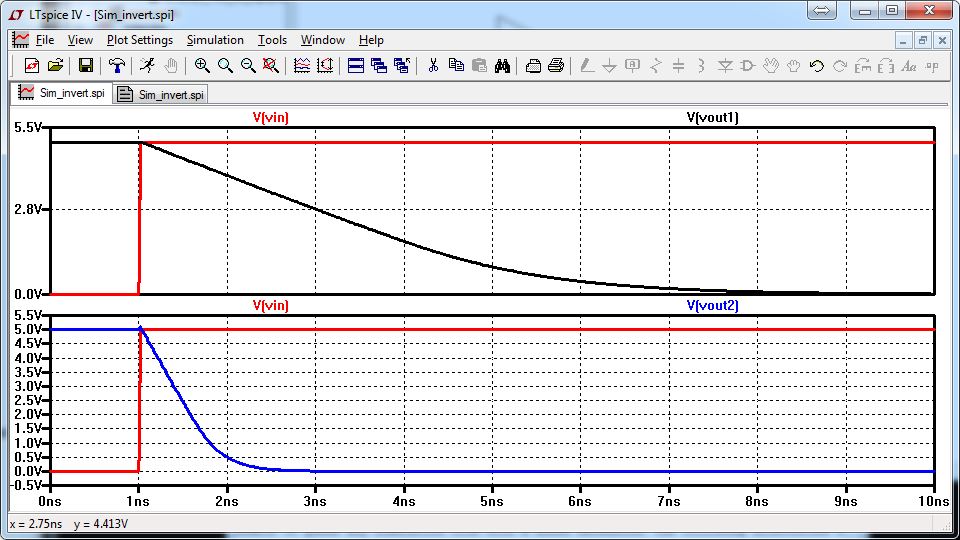
Vout1 or out_20_10 is the regular inverter.
Vout2 or out_100_50 is the parallel inverter.
Cap=100fF
Cap=1pF
Cap=10pF
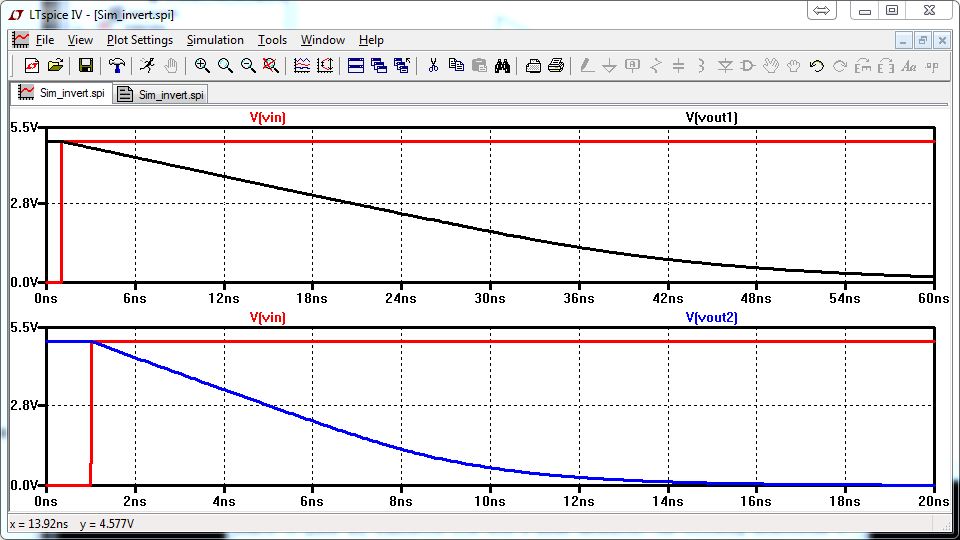
Notice that with larger capacities, the longer the delay is. And
that the parallel inverter is slightly quicker than that of the
none. This will affect the overall clock time in a larger
circuit.
Be sure to backup your files.
My Jelib File
More information can be found at cmosedu.com