Lab 4 - ECE 421L
Authored
by Matt Mumm, mummm2@unlv.nevada.edu
Sept 20, 2013
Lab
description
In
today's lab we will be making an NMOS and PMOS with schematics,
layouts, icons and simulations to get the I-V characteristics.
Make a new library for lab4.
Download the C5_models.txt for later use.
Making the NMOS as a schematic.
- Make a new schematic cell named NMOS_IV.
- Place an NMOS transistor under components -> schematic.
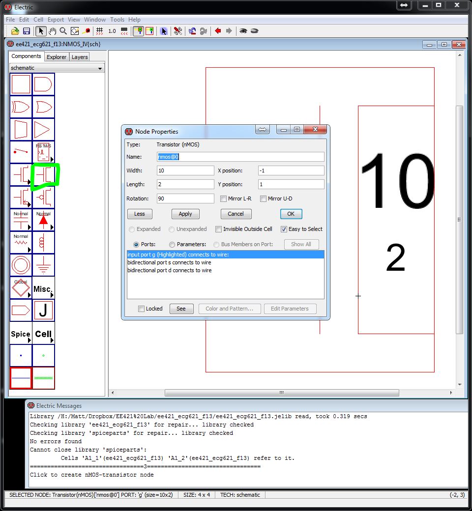
- Select the properties and change them to a width of 10 and length of 2.
- Change the model by selecting the NMOS and go to Tools -> Simulation (Spice) -> Set Spice Model
- Select the name and change it to NMOS
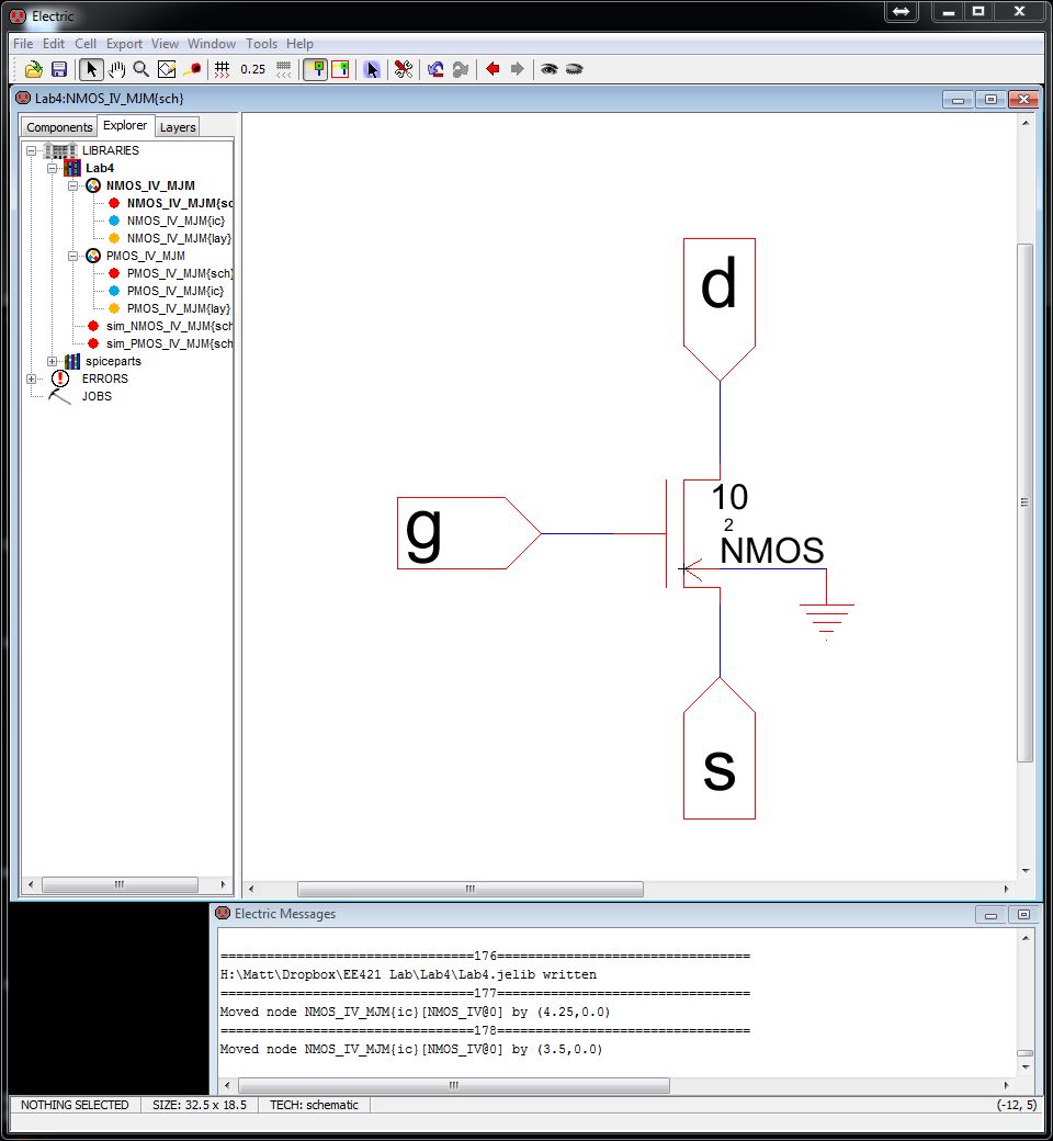
- Now simply place down the pins and export them as d, g, and s.
- Don't forget to place the ground (not connected to anything) and this will be used for the layout.
Your schematic should look something like this.
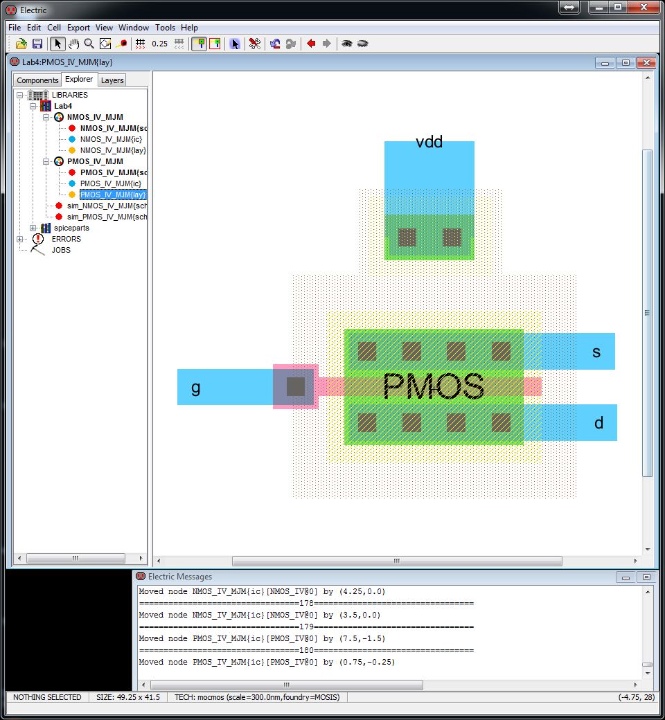
Now we are going to build the NMOS layout.
- Start by making a new layout cell with the same name as you used for the schematic.
- Place a NMOS under components -> mocmos.
- Select it and change the properties to a width of 10 and length of 2.
- While you still have the NMOS selected, go to Tools -> Simulation (Spice) -> Set Spice Model.
- Rename the spice model to NMOS.
- (DO NOT name the actual NMOS itselt!)
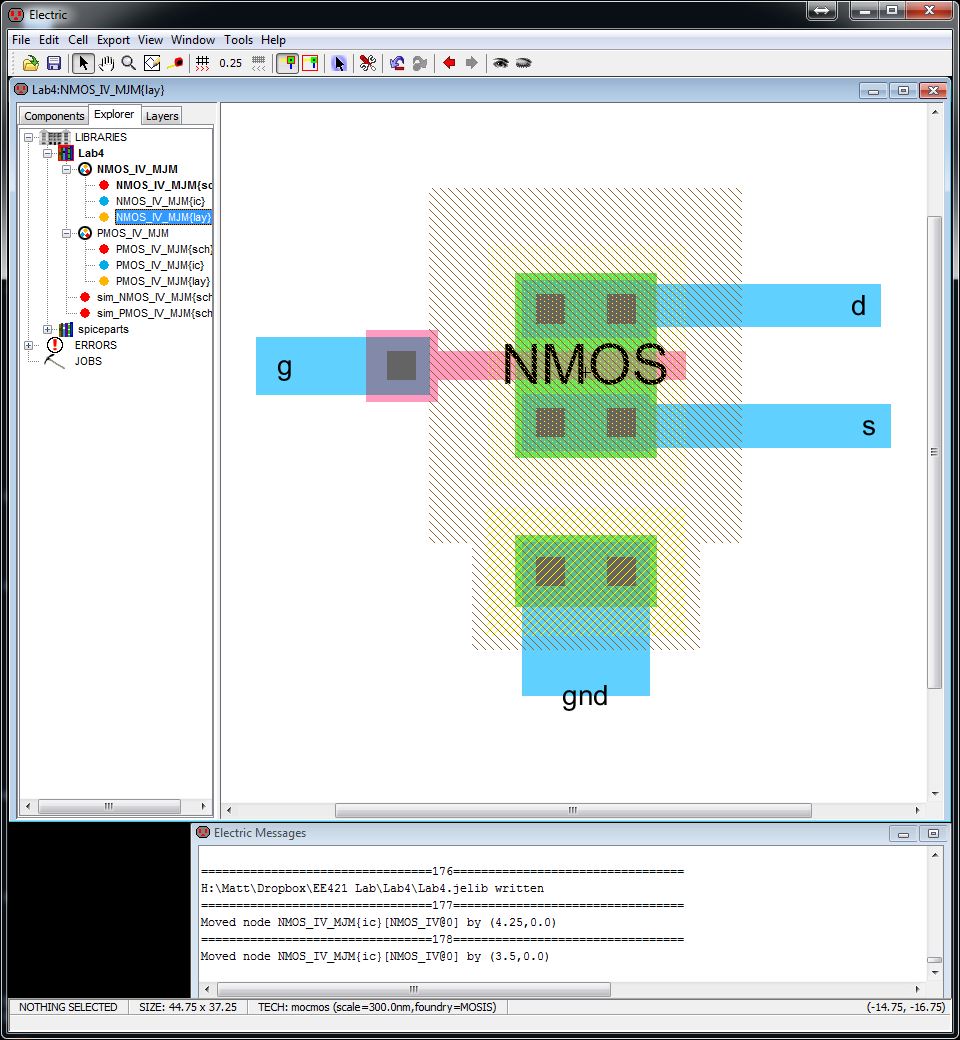
- Now
place a nAct above and below the NMOS. These will be used to
connect the drain and source. Change the width of them to 10
- Place the Metal1-Polysilicon connection next to the NMOS. (Pink/Purple box).
- Finally, place a pWell node and this will be used for ground. Change the width to 10
- Left
click - Right click to connect the nActs to the NMOS device. If
the width of the arc is not 10, change it. Also you can move the nActs
closer to the NMOS. (This will help reduce resistance)
- Select the polysilicon(pink) and connect the body of the NMOS to the M1-poly connection.
- Move the pWell node so that the pWell is touching the pWell of the other devices.
- Almost done... grab the metal 1 arc and add connections to the polysilicon connection, nActs and pWell devices.
- Your layout should look something similar to the image below.
- Finally
export (ctrl+e) the pins, not the arcs, as g, d, s, and gnd.
(Notice these are all lowercase to match the schematic. So
if you choose different names or uppercase, make sure the names match.)
- Check for any errors. DRC, NCC and Well checks.
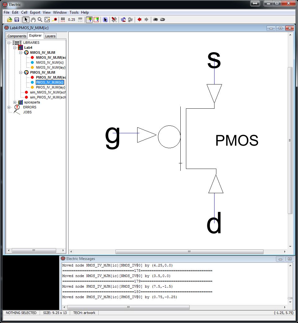
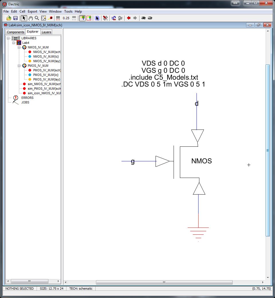
Making an Icon
You might need an icon if you wish to use these devices in a bigger circuit.
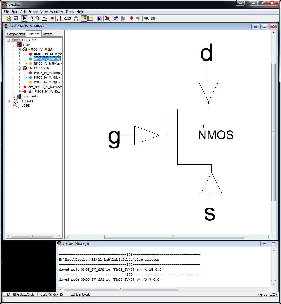
- Start by going to the schematic and selecting View -> Make Icon View.
- Select the new image that appeared on your schematic and hit ctrl+d (this brings you "down" into the icon)
- Now,
using all your amazing art skills, you can edit and manipulate the
image so it matches your transistor. Go ahead and delete the
ground connection, if it appeared.
- Don't forget to add some text to name your icon.
- You might have something that looks like the icon below.
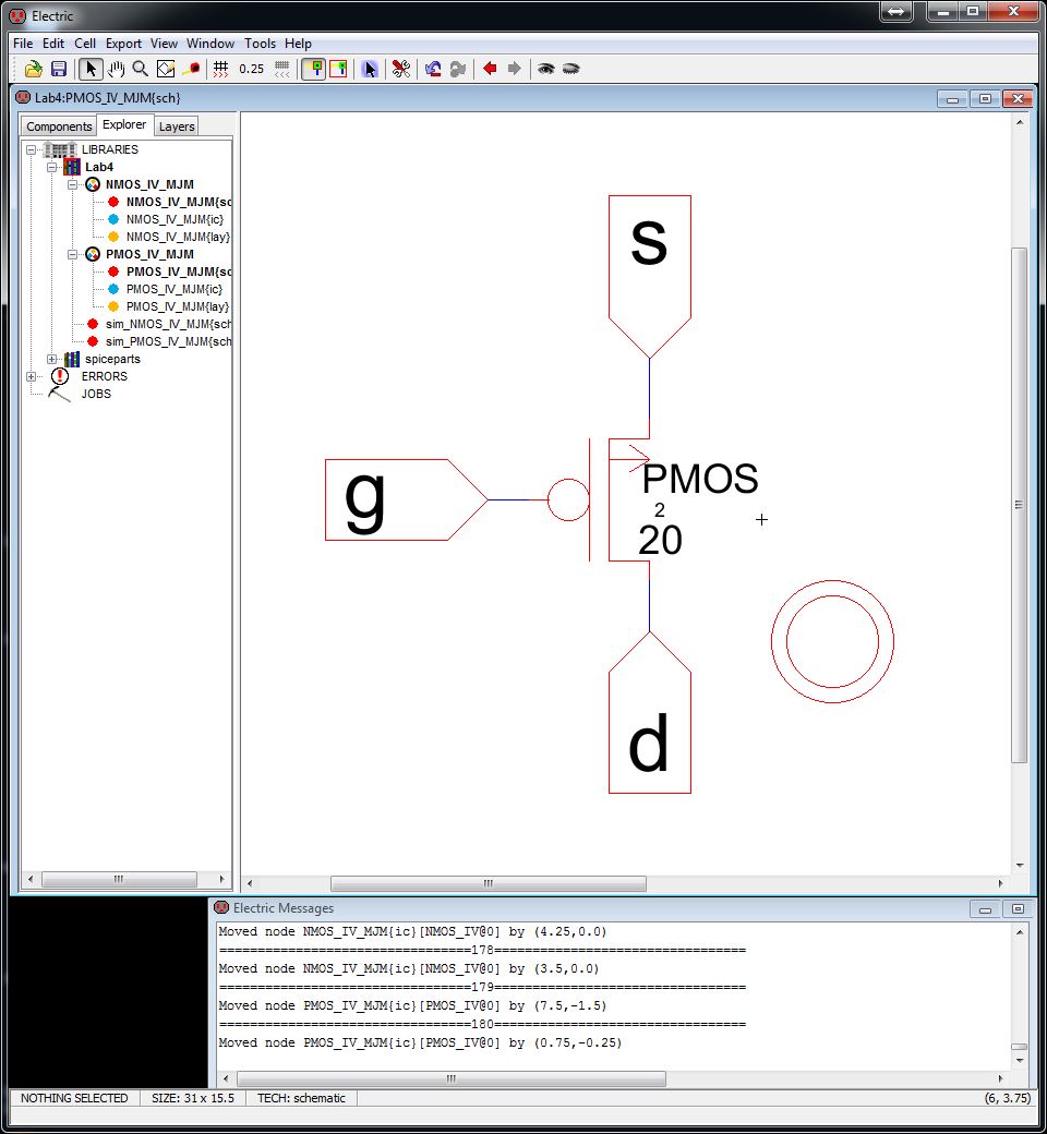
Making a PMOS transistor
You will be repeating the last 3 stages of instructions except for a few changes.
- Use PMOS, instead of NMOS (naming, spice modeling, selection of the transistors for schematic and layout.)
- Width of 20, length of 2
- nWell instead of pWell. (Power instead of ground)
- pActs instead of nActs for the source and drain.
- Add in a circle to your icon for gate connection.
Images for the PMOS can be seen below.
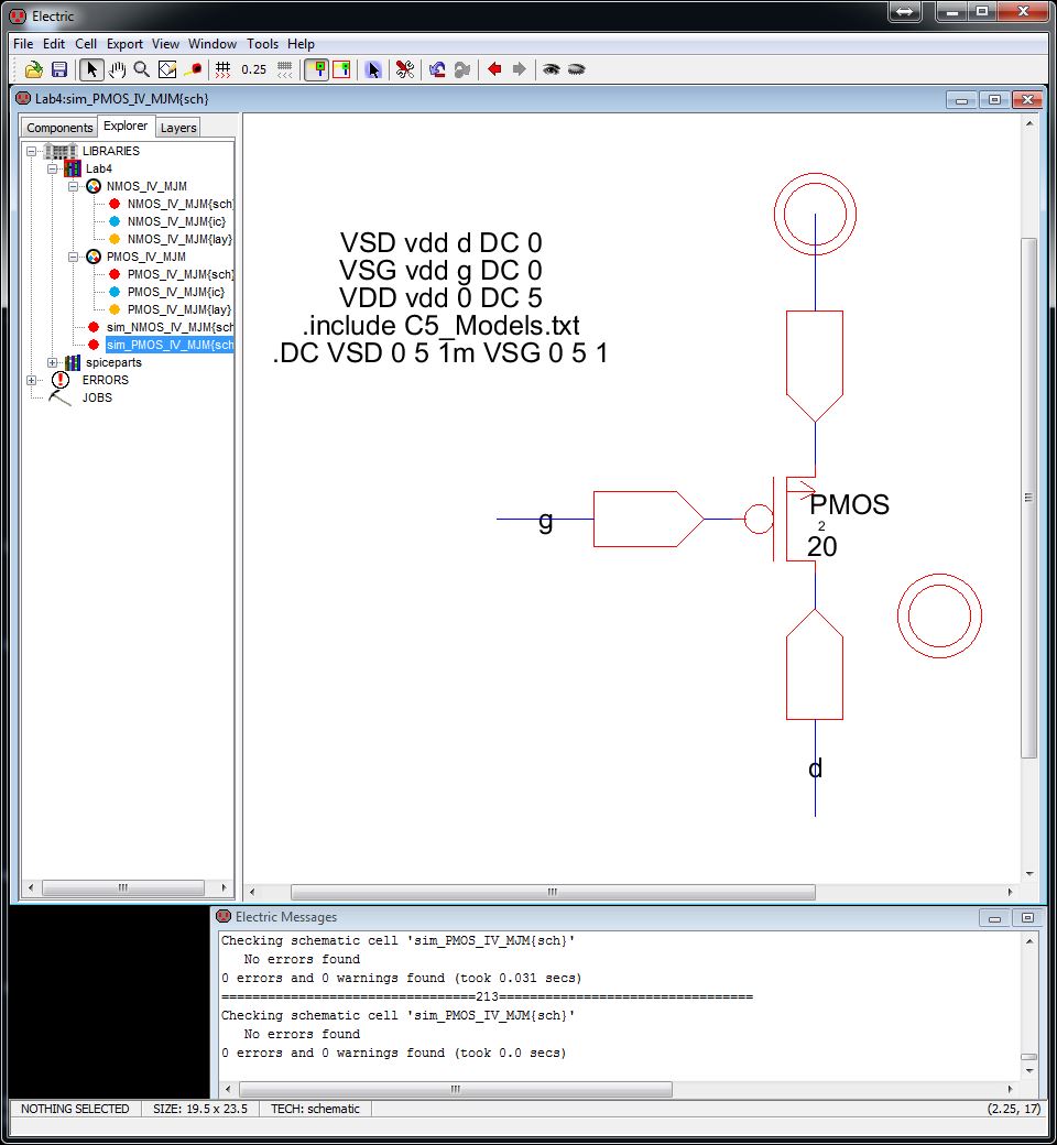
Making a simulation
- Two options:
- Either copy and paste your schematic OR
- Place your icon that you made
- No matter which option you choose, you should still be able to simulate.
- Add in the spice code (found under misc in components) seen below.
- Notice
there is no exporting in the simulation; this is because we are not
using the pmos in a hierarchy circuit. There is no need for it
here.
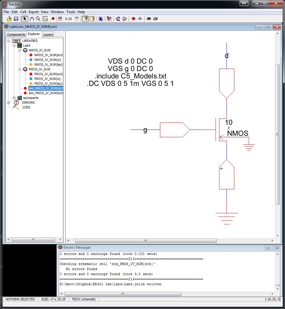
Simulation using an Icon
- arcs(wires) were added and labeled.
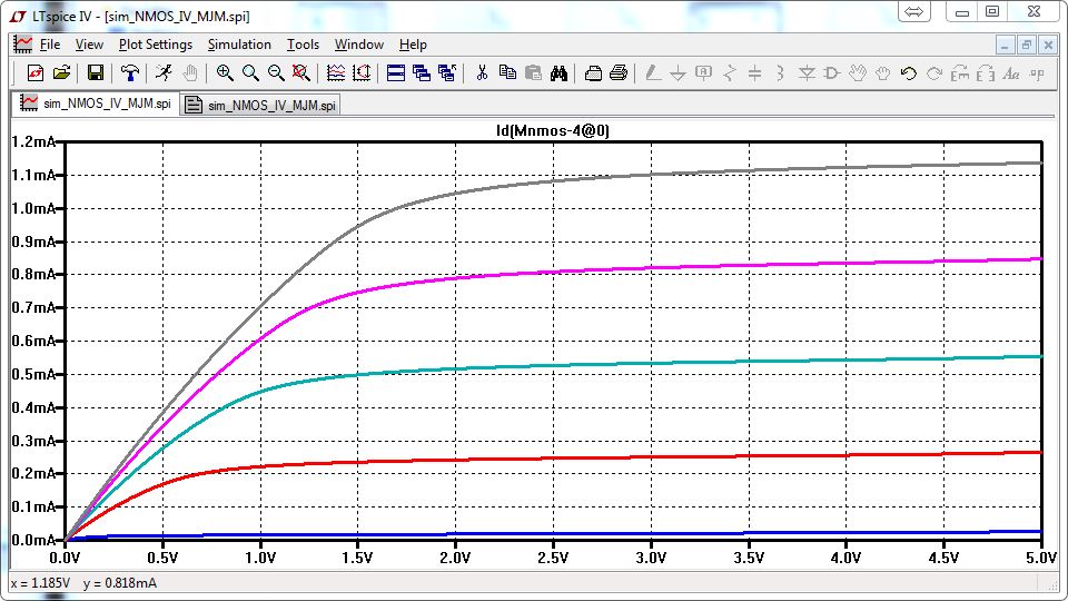
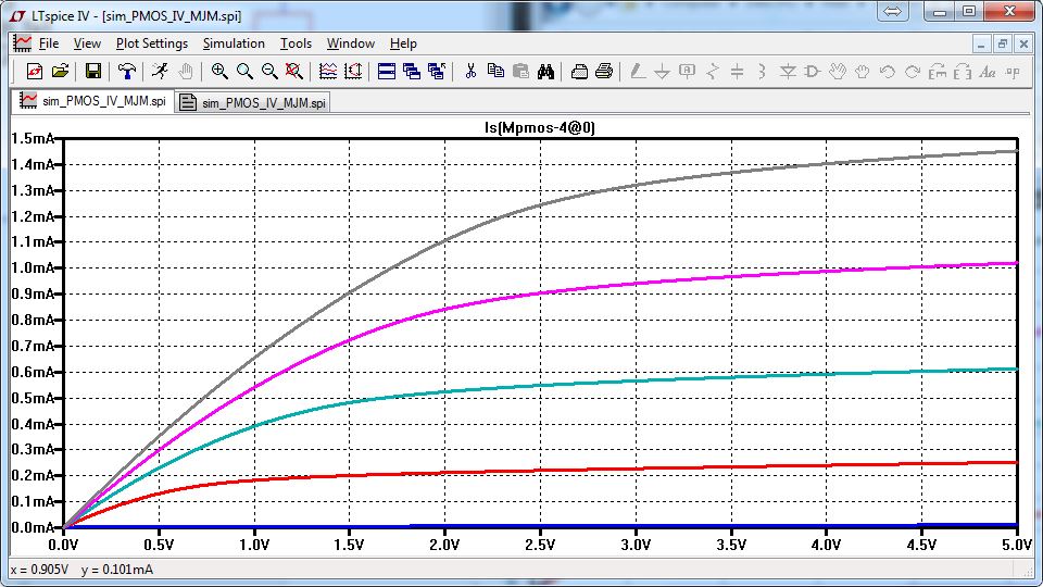
My simulation results.
Be sure to backup your files.
My Jelib File
More information can be found at cmosedu.com