Lab 2 - ECE 421L
Authored
by Matt Mumm, mummm2@unlv.nevada.edu
Sept 6, 2013
Today's Lab we will be going over the design of a DAC.
Pre-Lab:
1) First we need to get the proper library files. Download Lab2.jelib file, which contains a simulation example of a 10-bit DAC.
2) Open the newly downloaded library file and your course library file inside electric.
3) Go to Cell -> Cross Library Copy
4) You will want to copy over the sim_ADC_DAC{sch} into your course library.
5) Be sure to get all of its subcells, and all related views.
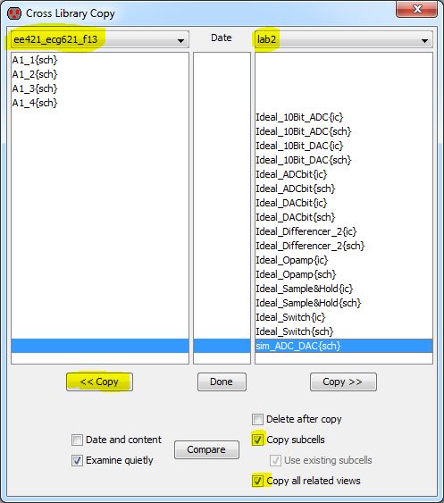
6) Hit done once the copy is complete.
7) Go ahead and close the lab2.jelib library, so that only one library is open, as seen below
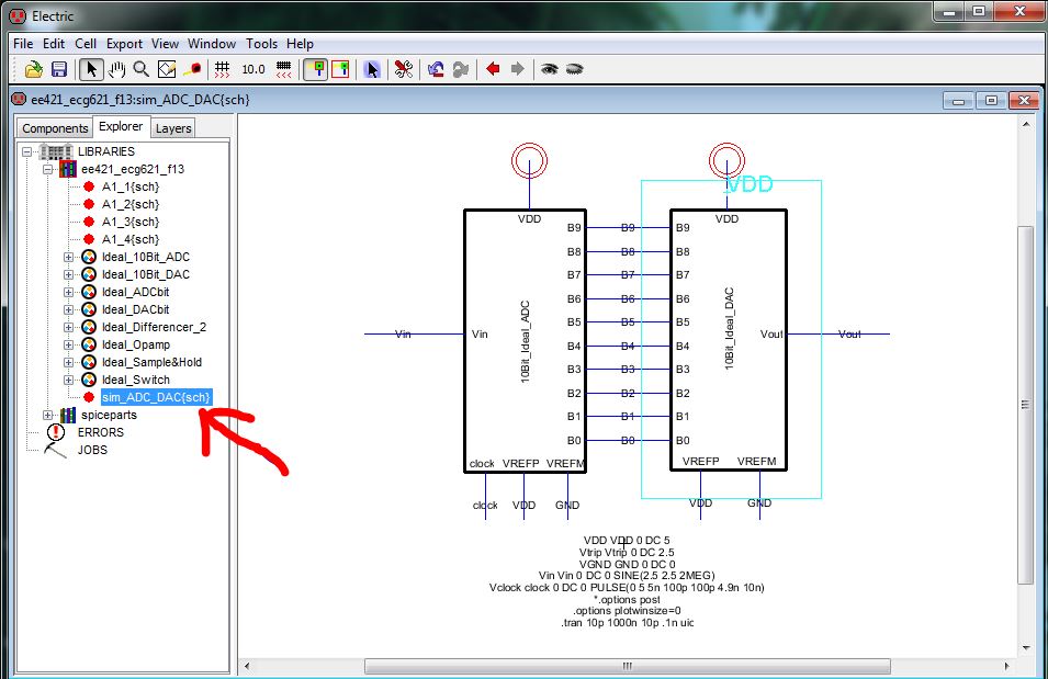
8) Go ahead and select the cell, sim_ADC_DAC{sch} and run it.
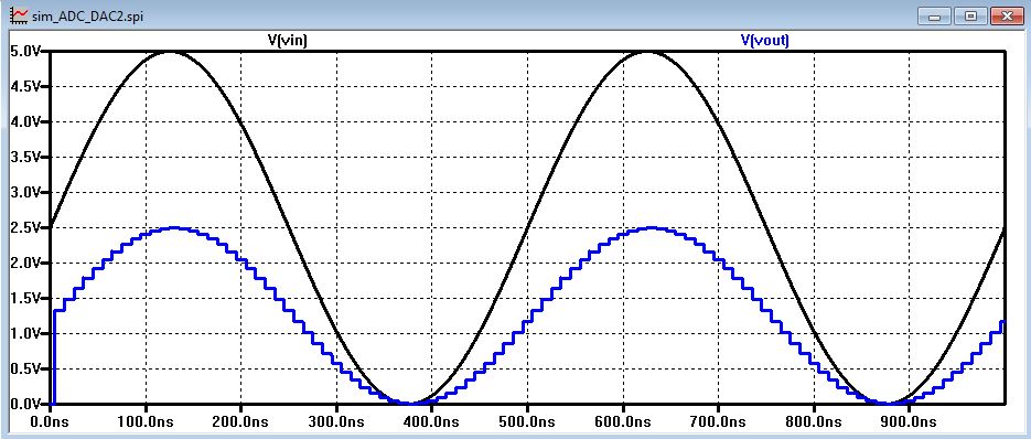
9)
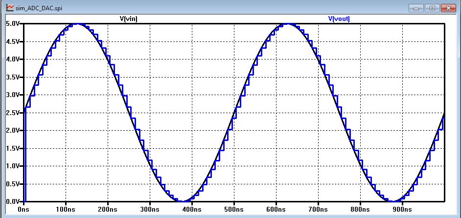
After LTSpice is loaded, go ahead and plot V(vin) and V(vout) under
Plot Settings -> Add Trace. You should get a graph that looks
like this below.
10) Be sure to save and backup your plots and libraries as you are working on the lab.
Lab
Today
we are going to take an ideal input signal from an ADC and convert it
back to analog. Doing this allows us to see how the signal
changes.
- First we need to build the DAC.
- Start by duplicating the cell Ideal_10bit_DAC and renaming it.
- Open the newly created cell Ideal_10bit_DAC and double clicking on the schematic (indicated by {sch})
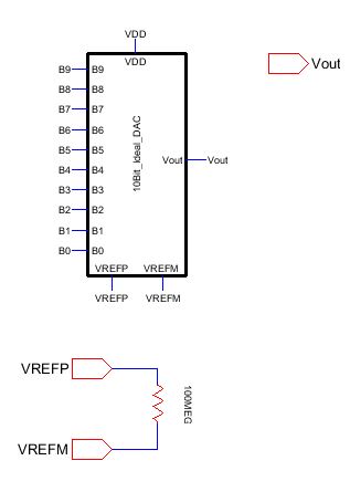
- Delete everything except the icon, VREFP pin, VREFM pin and Vout pin, as seen below.
- Now
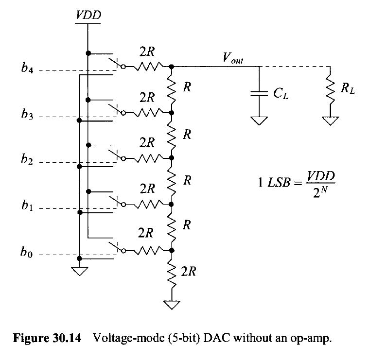
we will build the circuit, using N-well resistors. Since there are 10
input bits, we need 10 sets of resistors. The picture below only shows
a 5 bit input.
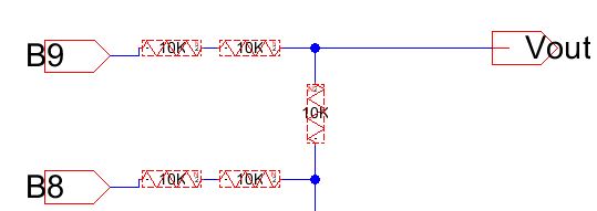
- Each
R will be 10K and to create 2R, you will need to put 2 resistors in
series. Do Not place any switches as pictured above. Ignore the
capacitor and resistor load for now, we will come back to that
later.
- What is the overall resistance of the circuit? Well start with the very bottom 2R in
parallel with 2R connected to b0, which is R. Moving up, the R between
b1 and b0 in series with the new R is 2R. Following this pattern
all the way up shows us the overall resistance is R.
- The pins can be located under components and within schematic on the drop down menu.
- The start of your circuit should look like this:
- Notice that the pins
appeared to be labeled, however this is not the case. They are
actually connections. In order to export them, you need to select
the pin and hit "ctrl+e" and a new window will appear. Label them B9 to B0. Do not worry any other options listed.
- When
connecting to the Vout pin, be sure to click on the flat side. If
you connect it to the arrow side, the program will think Vout is an
input, instead of an output.
- Be sure to create a separate pin, exported to "vdd", connected to a large resistance and then grounded.
- Again, make sure you connect the arrow end of vdd to the resistor.
- Make sure you check your circuit
- After you've designed and drafted your schematic check it using Tools -> DRC -> Check Hierarchically or just hitF5
- The
most common error, when drafting schematics, is extra pins (remove
extra pins using Edit -> Cleanup Cell -> Cleanup Pins Everywhere)
- Now that we have the DAC built, lets connect it to the ADC inside of sim_ADC_DAC{sch}
- Start by duplicating the cell, sim_ADC_DAC{sch} and renaming it.
- Delete the current DAC icon that is in there.
- Drag and drop the icon (indicated by the blue dot) of your new DAC, that you created above, where the old one was.
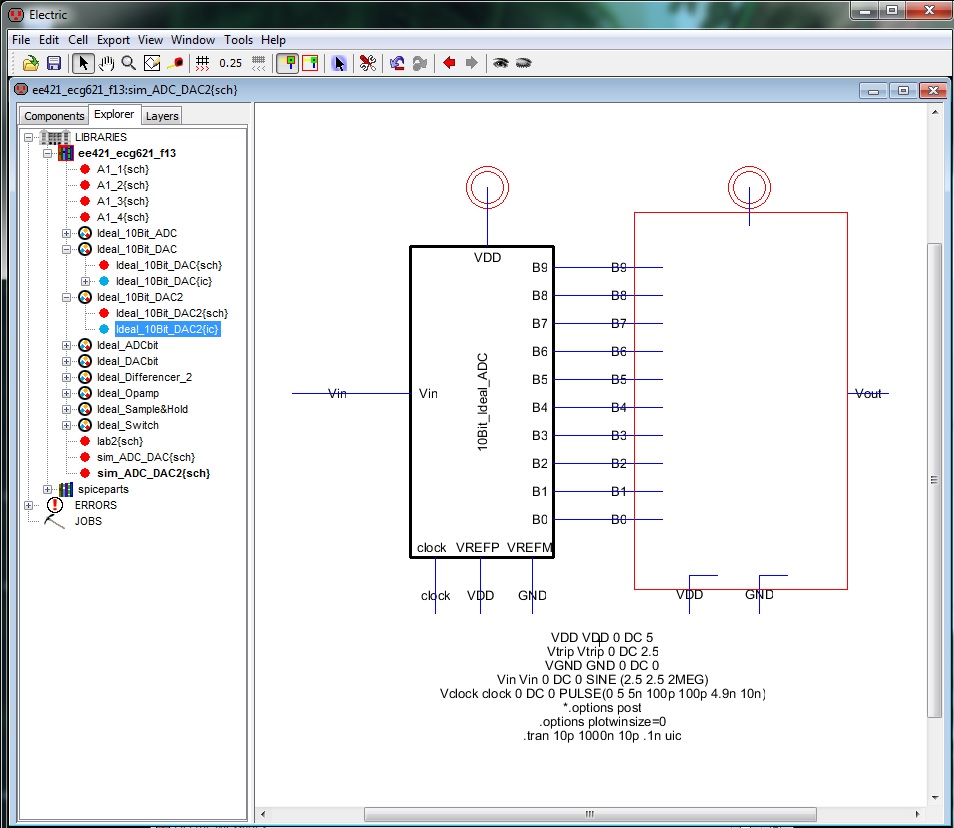
- Connect all the pins as they were before and be sure to check for errors.
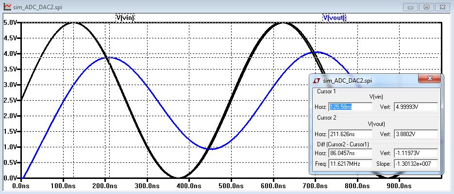
- Test and run your circuit. When plotting Vin and Vout, it should look exactly like the
3rd image on this page. Notice how Vout follows the same sinusoidal
pattern as Vin, but it has jagged edges and slightly off to the right.
This is due to the conversion.
- As the voltage increases to a certain point, the vout will also increase based on the equation 1LSB =(Vpos-Vneg)/(2^n).
- Example:
For a 3bit system with vin=1, N=3; the LSB will be 1/(2^3)=1/8.
If B1 is given an input of 1V and all other bits are grounded
(010) which is decimal 2. Then 2*LSB=1/4.
- Creating an icon for your DAC
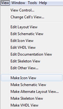
- Once you have your schematic complete, we can easily add in an icon by clicking on View -> Make Icon View
- A box will appear with the name of your schematic and all your pins connected to it.
- Clicking on the new icon and hitting "Ctrl+D" will bring you to the icon. Now you can edit it.
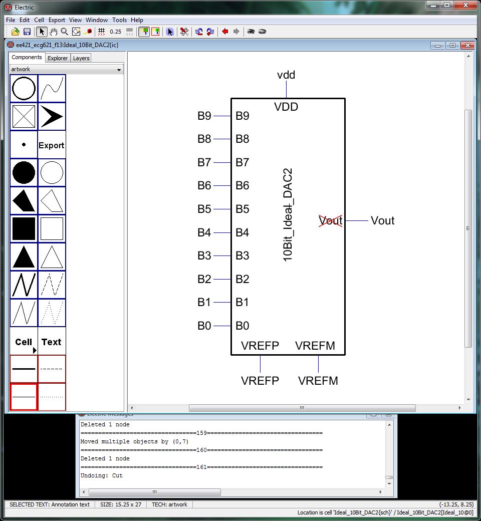
- Move the pins arround as you need to, go into components ->artwork to add other shapes or anything else want to do.
- Make sure to save as you go along.
- Duplicate your sim_ADC_DAC{sch} and rename it.
- Go ahead and delete the ADC portion.
- Ground the inputs B0 to B8. Connect Vin to B9.
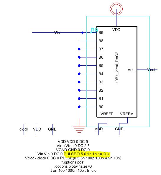
- We will need to change the sine function to a pulse function, as seen highlighted above.
- Now go to your DAC schematic and add in a capacitor, 10pF, between Vout and the resistors. Ground the capacitor.
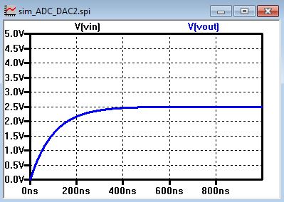
- Finally, running your simulation will give you a graph of charging a capacitor and you can calculate the delay time.
- Td=0.7*RC=0.7*(10^4)*(10x10^-12)=70ns
- Capacitance Load
- Use the circuit made above but with a sine wave input. You can see the phase difference between the input and output
- Resistor Load
- Replace
your capacitor with a resistor, 10k, and this time we can see the
amplitude is in half due to the resistive divider we just created.
- RC Load
- Finally,
place a capacitor and resistor in parrallel. We can see the
amplitude has changed and a phase shift has occured.
What
if the switches, seen in the schematic near the top, are not small
compared to R? There will be a voltage drop across the switches,
which will lower your overall output and cause your output not to be as
smooth.
Make sure to save and backup all your information
My Jelib File
More information can be found at cmosedu.com