Lab 6 - Design, layout, and simulation of CMOS NAND/NOR/XOR gates and a full-adder
Authored by Nolan Moore
Date: October 14, 2013
Email: mooren14@unlv.nevada.edu
Lab 6 Directions
Lab 6 Working Library
Prelab:
N/A
Lab Procedure:
Layout/Schematics
For this lab we will be designing and simulating CMOS logic gates. We will begin with a NAND gate, followed by NOR and XOR. A schematic, icon and layout will be created for each gate, and a simulation showing proper operation will be performed for each. Lastly we will create full adders using our CMOS gates. The first adder will be created using all 3 gates, and the second adder will be created using only NAND and XOR gates.The layout for each gate will use a standard frame, or S-Frame, to make each gate compact and standardized, allowing for easy ground and power routing. The S-Frame to be used can be seen below.
S-Frame Layout View

NAND gate
The NAND gate will be created with 10/2 PMOS and NMOS transistors as seen in the following schematic. Additionally, the icon, created using circles and polygon lines, can be seen.NAND Schematic and Icon View
NAND Layout View

NAND Error Check Pass

NAND Simulation Schematic

In both the LTspice and IRSIM simulations, the logical operation of the gate is correct.
NAND LTspice Simulation

NAND IRSIM Simulation

NOR gate
The schematic for the NOR gate is below. The PMOS are now 20/2 and the NMOS are 10/2, just as we had with the inverters in previous labs. The icon is below as well. NOR Schematic and Icon ViewNOR Layout View

NOR Error Check Pass

NOR Simulation Schematic

In both the LTspice and IRSIM simulations, the logical operation of the gate is correct.
NOR LTspice Simulation

NOR IRSIM Simulation

XOR gate
The schematic for the XOR gate can be seen below. On the left are two inverters while the right half contains the majority of the XOR gate. As with the NOR gate, the PMOS are 20/2 and the NMOS are 10/2. The icon for the gate can also be seen.XOR Schematic and Icon View
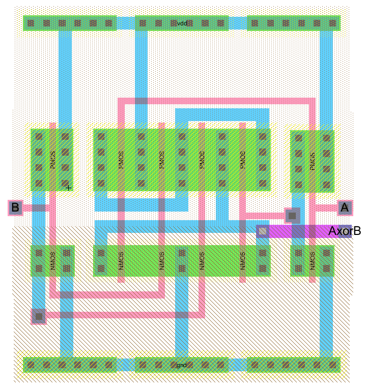
As seen in the layout below, 3 S-Frames were used to contain the XOR gate. The ground and power rails in each frame were connected together. The external nodes A, B and AxorB are all connected to Metal 2 pins.
XOR Layout View
XOR Error Check Pass

XOR Simulation Schematic

In both the LTspice and IRSIM simulations, the logical operation of the gate is correct.
XOR LTspice Simulation

XOR IRSIM Simulation

Full adder 1
Full Adder with NAND, NOR, and XOR gates - Schematic
Full Adder with NAND, NOR, and XOR gates - Icon View
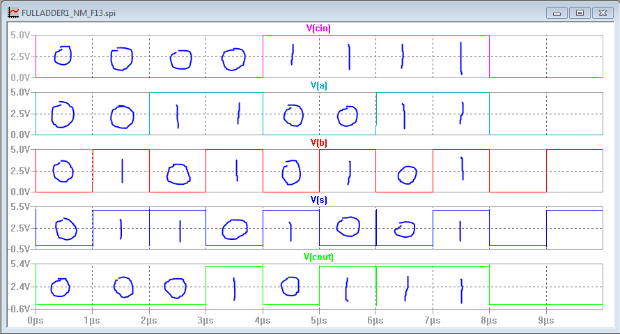
In both the LTspice and IRSIM simulations, the logical operation of the full adder is correct.
Full Adder with NAND, NOR, and XOR gates - LTspice simulation
Full Adder with NAND, NOR, and XOR gates - IRSIM simulation

Full adder 2
The second full adder design features 3 NAND gates and 2 XOR gates as seen in the schematic seen below. The icon for this full adder is the same as the one used for the previous full adder and as such will not be included here.Full Adder with 3 NAND and 2 XOR gates - Schematic

The inputs and output for the full adder layout are on Metal 2.
Full Adder with 3 NAND and 2 XOR gates - Layout

The LTspice simulation for the second full adder design can be seen below. The logical operation is correct.
Full Adder with 3 NAND and 2 XOR gates - LTspice simulation

Return Home