Lab 5 - Design, layout, and simulation of a CMOS inverter
Authored by Nolan Moore
Date: October 4, 2013
Email: mooren14@unlv.nevada.edu
Lab 5 Directions
Lab 5 Working Library
Prelab:
N/A
Lab Procedure:
Layout/Schematics
For this lab we will be designing and simulating CMOS inverters. We will explain the layout and schematics used for a standard 20/10 (the first number, 20, being the width of the PMOS and the second, 10, being the width of the NMOS) inverter as well as a 100/50 inverter.Draft schematics, layouts, and icons for inverters having drawn sizes of:
20/10 (= width of the PMOS / width of the NMOS with both devices having minimum lengths of 2)
100/50 where the PMOS is 20/2 with M = 5 (5 MOSFETs in parallel to get 80 and 40, set multiplier as seen below)
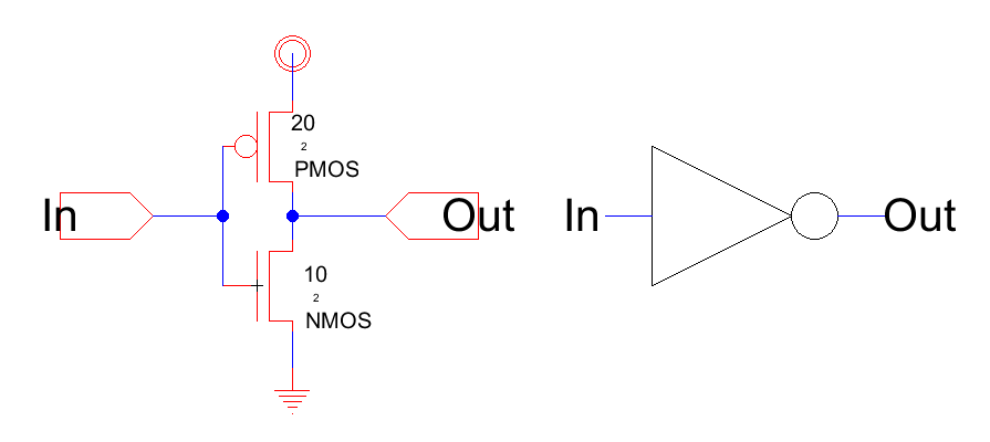
Below is a screenshot of the basic 20/10 CMOS. The design uses the layouts created in lab 4 with the inverters rotated 90 degrees. Connected to the left side of the PMOS (the source) is a large vdd connection to Metal 1. Similarly, the left side of the NMOS (the drain) is connected to ground. The PMOS and NMOS are connected together on the right with an output pin. The gates are connected together and attached to an input pin. Being a 20/10 inverter, the PMOS has a width of 20, double that of the NMOS. This is necessary because the PMOS is generally weaker than the NMOS. Doubling the width allows more current to flow, making it as effective as the NMOS.

The schematic and icon for the 20/10 inverter is below. The schematic consists of very few components, and features In and Out nodes. The icon was created using geometric shapes and represents a basic inverter.
The 100/50 inverter is based off of the design of the basic 20/10 inverter. The PMOS and NMOS are copied horizontally 4 times, and space efficiency is maximized by having the inner P-active and N-active connections connect to two separate PMOS and NMOS transistors, respectively. The alternating

The schematic and icon for the 100/50 inverter is essentially the same as the schematic for the 20/10 inverter. The only difference is that a multiplier of 5 for both the PMOS and NMOS were added, and "100/50" was added to the icon.

SPICE Simulation
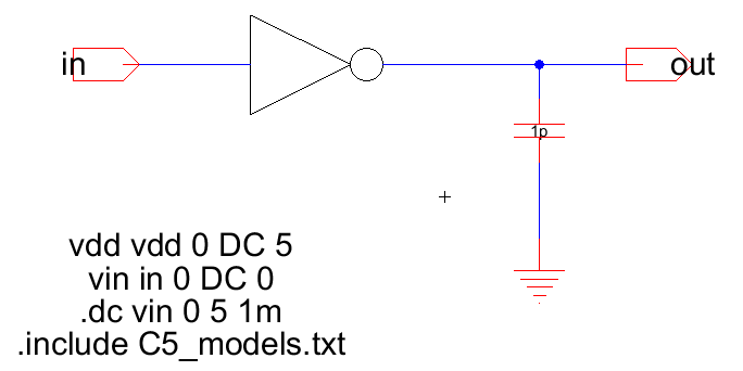
We will begin running simulations on both of our inverters, starting with basic SPICE DC sweeps. We will be measuring both the input as it rises from 0V to 5V and the output of the inverter. Because this is a DC sweep analysis, time will not be factored into the results and capacitors will be simulated as open circuits, negating their importance and effect on the simulation. As such, we will only post a screenshot of the 20/10 inverter with 1pF load and 100/50 inverter with 1pF load. However, the only difference between these two inverters is the size of them, meaning that both sims will feature identical results.The schematic for the 20/10 inverter simulation with SPICE code can be seen below. The 100/50 schematic is identical except that the icon of the 20/10 inverter is replaced with the 100/50 icon. As such, the screenshot of the 100/50 simulation schematic will be omitted.
Schematic of CMOS inverter SPICE simulation

20/10 CMOS inverter with 1pF capacitor load
100/50 CMOS inverter with 1pF capacitor load

As mentioned previously, the capacitors had no effect on these simulations, and the difference in sizes of the inverters was also negligible. As such, the results of all the SPICE simulations were identical, and we can see two representing screenshots above.
ALS Simulation
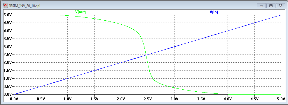
Next, we will perform simluations using ALS, or Asynchronous Logic Simulator. ALS is designed to simulate digital logic on an "upper level," simply seeing the 20/10 and 100/50 inverters as just inverters. Because of this, both inverters simulated will provide identical results. The load capacitors do not play a part in changing the delays seen in the results of the sims. Because the results of the ALS simulations will be identical, we will only show a single simulation for the 20/10 1pF inverter and the 100/50 1pF inverter.For these simulations, we simply created a clock pulse with a period of 30ns on the input of the inverter. The output signal can be seen below the input signal. The "main" cursor is set at 0ns and the "external" or secondary cursor is placed at the time where the output reacts to the input, allowing us to measure the delay.
Again, we show a screenshot of the simulation schematic before the simulation results. It is very similar to the schematics used for the SPICE sims except that off-page nodes have been added to the input and outputs of the inverters. Also as previously mentioned, the schematic for the 20/10 inverter simulation will be shown as the 100/50 simulation simply switches the icon.
Schematic of CMOS inverter for ALS and IRSIM simulations
20/10 CMOS inverter with 1pF capacitor load

100/50 CMOS inverter with 1pF capacitor load

As we can see from the results of the simulations, the delta/delay for both inverters was 10.28ns.
IRSIM Simulation
Finally, we will perform simulations using IRSIM. Unlike the results of the previous simulations, we will see differing results for each digital circuit simulated. As mentioned previously, we will be using the schematics used in the ALS simulations.20/10 CMOS inverter with 100fF capacitor load

20/10 CMOS inverter with 1pF capacitor load

20/10 CMOS inverter with 10pF capacitor load

Simulation results for 20/10 CMOS inverter:
100fF load: 0.257ns
1pF load: 2.243ns
10pF load: 22.628ns
We can see that as the size of the capcitor load increases, the delay of the inverter increases as well. In fact, the delay appears to multiply at the same rate as the capcitance.
100/50 CMOS inverter with 100fF capacitor load

100/50 CMOS inverter with 1pF capacitor load

100/50 CMOS inverter with 10pF capacitor load

Simulation results for 100/50 CMOS inverter:
100fF load: 0.234ns
1pF load: 2.336ns
10pF load: 22.628ns
Again, we see the linear rising of the delay and capcitance of the load. In addition, the delays appear to be slightly smaller than those of the 20/10 inverter simulations. This could be due to user or technial errors as we were unable to properly set the graph markers to exact values for measurement.
Return Home