Lab 3 - Layout of a 10-bit digital-to-analog converter (DAC)
Authored by Nolan Moore
Date: September 13, 2013
Email: mooren14@unlv.nevada.edu
Lab 3 Directions
Lab 3 Working Library Download
Lab Procedure:
In Lab 2, we created an "R-2R" DAC and the associated schematic and icon. We tested the DAC under various types of loads, including a resistor load, a capacitor load, and an RC load. Now we will create the basic layout cells for the schematic.
To recap, we will use N-Well resistors to form the individual cells in the 10 bit DAC. Each cell will consist of an input L, two 10k resistors connecting the input to the output, the output R, and another 10k resistor from R to ground.
Schematic of R-2R N-Well resistor

The resistors used will be 10k Ohms. sheet resistance of 800 Ohms per square. Since the first lab, we have been using the design rules for ON Semiconductor’s C5 process and fabrication through MOSIS. The documentation and rules for this specific process can be found here. According to the design rules, the minimum width of the N-wells should be 12 lambda, or 3.6 microns. Using this value and the formula for well resistance, we can calculate the required length of the resistor:
N-Well Resistance Calculations

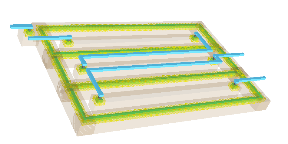
As seen in the following picture, each N-well resistor will be layed out in parallel, allowing for maximum space savings. Though it may appear that the metal arcs (blue, Metal-1) intersect with the P+ guard rings, they actually rest at a higher level above the substrate.
To reduce subtrate noise in the design, we can surround each N-well resistor with a P+ (P-active) guard ring. This set of rings is connected to ground in the upper left corner of the layout near the input. Below is the layout with gaurd rings added as well as a 3D view of the layout.
Layout 2D View

Layout 3D View
Of course, it is necessary that we check to ensure that the layout has no design errors and is properly associated with the schematic that we design previously. Below are screenshots of the DRC, NCC, and ERC checks performed on the layout and schematic.
Layout DRC Check

Schematic DRC Check

Layout and Schematic NCC Check

Layout ERC Check
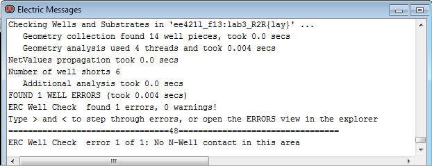
As we can see in the ERC, or Electrical Rule Checking, check, we had one error, stating "No N-Well contact in this area." The reason for this error is that the N-well in which the P+ guard ring rests requires an N-well contact. This issue was fixed by changing the gnd contact from a P+ contact to an N-well contact.
The library file used for this lab can be downloaded here. The layout for the R-2R cell is located under the "lab3_R2R" cell group.
Return Home