Lab 2 - R-2R 10-bit Digital-to-Analog Converter (DAC) - Schematic Design
Authored by Nolan Moore
Date: September 6, 2013
Email: mooren14@unlv.nevada.edu
Lab 2 Directions
Prelab:
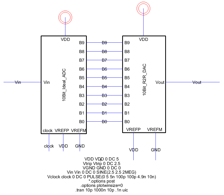
To begin, open Electric and create a new library, if you haven't done so already. You can find the New Library option under the File menu. For this prelab, we will be using a analog-to-digital converter simulation example found in lab2.jelib. Open lab2.jelib and go to Cell > Cross Library Copy... Here, choose sim_ADV_DAC{sch} from lab2 and copy it to your current library. Be sure that "Copy subcells" and "Copy all related views" are checked at the bottom of the window. Click done to add the cell to our library.

Double clicking the newly added "sim_ADC_DAC{sch} file in your library will open the schematic cell. You should see it shown in your main window, as seen below.

Next, we will run the simulation. Before continuing, ensure that LTSpice is installed on your computer and that the program location in Electric Preferences has been configured. When everything is ready, go to Tools > Simulation (Spice) > Write Spice Deck... to run the simulation. The LTSpice siumulation window should appear. Nothing will currently be visible in the graph except for the grid. We will add our traces to the graph under Plot Settings > Visible Traces. Choose both vin and vout and you should see a graph shown below.

Discussion
Setting the fequency of the AC input signal to 4 MHz (double from the original 2 MHz) creates an expected result in the simulation results.


Lab Procedure:
We will create a 10-bit DAC using a resistor ladder. This particular type of DAC is known as an R-2R DAC because the ladder steps will be built from resistors of R and 2R value. R will be 10k and 2R will be two 10k resistors in series.

For this schematic, we created a new icon from scratch. The individual pins were already exported, so making a new icon was very simple. Under the View menu, we simply clicked Make Icon View to create the new icon. This does not automatically replace any old copies of the icon in schematics and must be done manually.
![]()
Looking at the resistor ladder, one would think that determining the output resistance of the DAC would be a difficult and arduous task. However, as seen in the following image, this process is actually fairly easy when we start from the bottom and work our way up.

Next we will see how our DAC performs when connected to a capacitor load of 10pF. The lower 9 bits of the DAC will be connected to ground, or logic 0, and the uppermost bit will be connected to a DC pulse voltage source (as seen below).

There will be a delay created by the charing of the capacitor. The time delay should be equal to 0.7RC. As seen previously, our output resistance is 10k Ohms, and the capacitor is 10pF. This means that the time delay should be about 0.7 * (10^4 * 10^-11) or about 70ns. We can see the hand calculations done below.

The results of the simulation can be seen below. At about 70ns, Vout is equal to about 3.75V, halfway between the starting voltage of 2.5V and the full 5V.

Next we want to ensure that the DAC we created works as functioned. We replace the Ideal DAC in our test schematic with our R-2R DAC. You can see the full schematic below.
The simulation results show that the output waveform is nearly identical to the one created during the prelab.

Next we will observe how the DAC performs when driving different loads. The first load will be a single 10k resistor. Notice that the output waveform is half the size of the original input waveform. The reason for this is because the output resistance of the DAC is also 10k. The two 10k resistors function as a voltage divider, cutting the wave amplitude in half.

With a single capacitor load of 10pF, we see a delay and an associated drop of amplitude.

With a capacitor load of 10pF and a 10k resistor in parallel, we see a similar delay as with the single capacitor load, but we also see the amplitude cut as seen with the single resisotr load.

Lastly, we would like to examine what would happen in a real world situation where MOSFET transistor are used as switches providing the data bits to the DAC. These switches will have some non neglible resistance that must be accounted for when designing the DAC. If the resistance of the switches is not small in comparison to the value R used in the DAC, then there will be a drop in the output voltage at each bit. This will result in a lower voltage for the final output voltage. This will be a lower voltage than the source voltage and could cause inaccuracies in the conversion.
Return Home